Welcome to Surface Mount Process
The hub for Surface Mount Technology
|
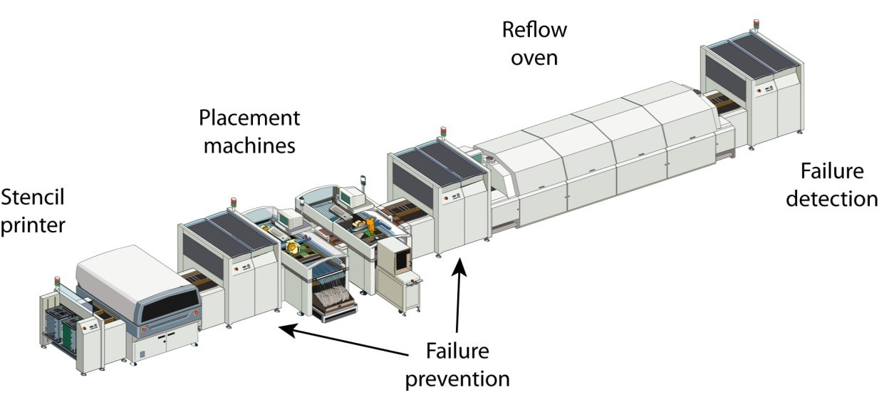
This website has been created primarily to be a technical resource for surface mount process engineers and also for anyone with an interest in surface mount technology (SMT). The scope of the website will be all aspects of the manufacturing process from solder paste printing, solder paste inspection, component placement, reflow soldering through to automatic optical inspection (AOI) and will include answers to the many frequently asked questions.
|
Introduction to Surface Mount Technology
|
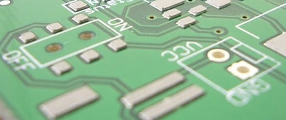
Surface Mount Technology is an area of electronic assembly used to mount electronic components to the surface of the printed circuit board (PCB) as oppose to inserting components through holes as with conventional assembly. SMT was developed to reduce manufacturing costs and also to make more efficient use of PCB space. As a result of the introduction of surface mount technology it is now possible to build highly complex electronic circuits into smaller and smaller assemblies with good repeatability due to the higher level of automation.
What are SMD's?
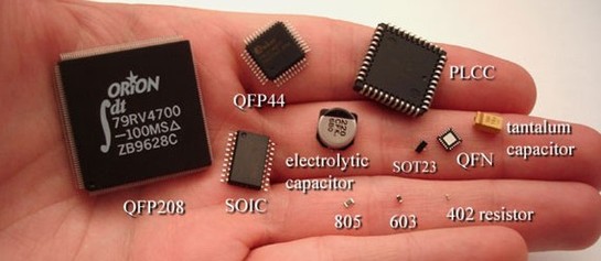
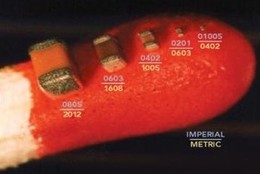
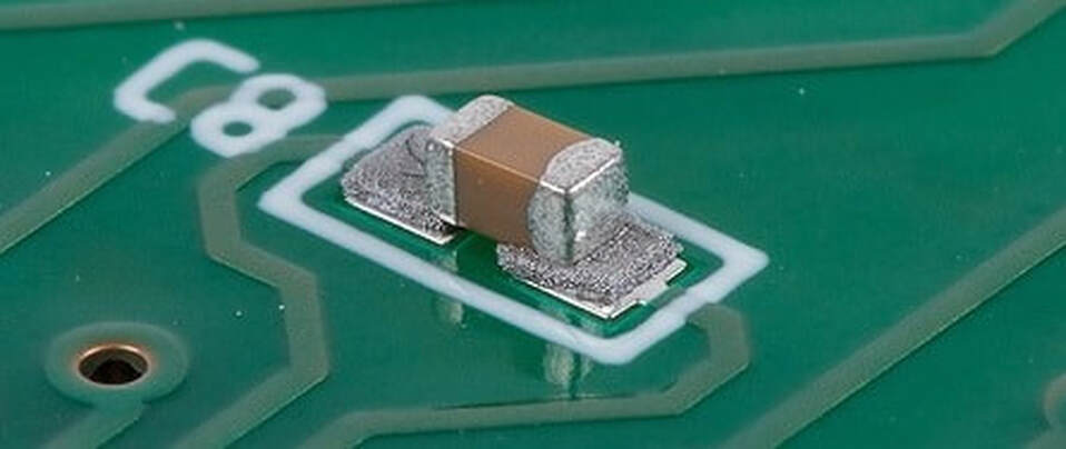
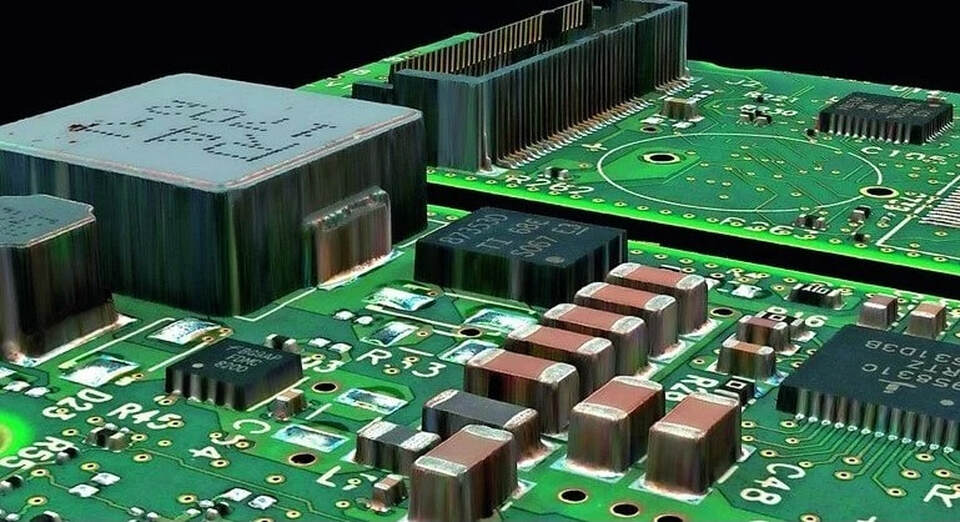
Surface mount device or SMD is the term used for the electronic components used within the surface mount assembly process. There is a wide range of SMD component packages available on the market and come in many shapes and sizes - a selection can be seen below:-
Surface Mount Assembly Process
The smt process starts during the design phase when the many different components are selected and the PCB is designed using a software package such as Orcad or Cadstar (others are available).
It is important to realise that the process starts at this stage as this is the best time to incorporate as many design features as possible that will make production straight forward and head-ache free. Quite often circuits are taken from the schematic design phase to PCB layout with the main considerations being the functionality, which of course is very important, but design for manufacture and assembly (DFMA) should ideally be incorporated.
Once the PCB design has been finalised and components selected the next phase is to send the PCB data away to a PCB manufacturing company and components bought in the most suitable way to facilitate automation. The PCB panel design should be considered and specification created including PCB surface finish to ensure that the format that the PCB's are received is as expected and suitable for the machines to be used.
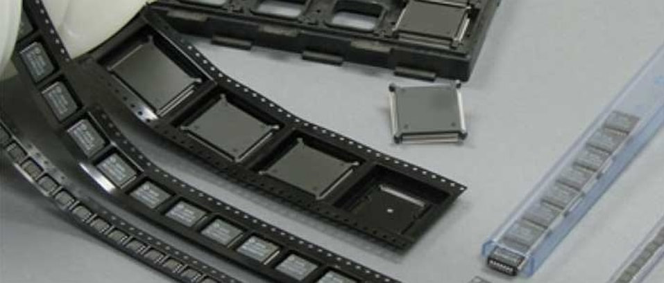
Components are available packaged in many different ways such as on reels, in tubes or in trays as can been seen below. Most are available on reels which is preferred but sometimes due to 'Minimum Order Quantities (MOQ's)' components are quite often supplied in tubes or in short strips of tape. If components are supplied in tray but tape is preferred, there are companies that provide the service to transfer from tray to tape following the industry standards. It is possible Both of these packaging types can be used but do need appropriate feeder types. Components supplied loose in bags should be avoided if possible as can lead to hand placements or the need for special feeding plates.
IPC - The Global Association for Electronics Manufacturing
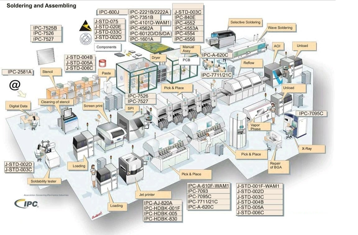
As in most industries, there are standards governing the many different processes for surface mount assembly. For the electronics industry, IPC was founded in 1957 as the Institute of Printed Circuits. Its name was later changed to the Institute for Interconnecting and Packaging Electronic Circuits to highlight the expansion from bare boards to packaging and electronic assemblies. In 1999, the organization formally changed its name to IPC with the accompanying tagline, Association Connecting Electronics Industries. There are various IPC standards that govern different aspects of electronics manufacturing and some can be seen below - More can be seen here.
Machine programming - Gerber / CAD to Centroid / Placement / XY file

Having received the PCB panels and components the next step is to setup the various machines used with the manufacturing process. Machines such as the placement machine and AOI (Automated Optical Inspection) will require a program to be created which is best generated from CAD data but quite often this isn't available. Gerber data is almost always available as this is the data required for the bare PCB to be manufactured - can be viewed using software listed here. If Gerber data is the only data available then the creation of the centroid / component placement list (CPL file) / XY file can be very time consuming and so Surface Mount Process offer the service to generate this file.
Solder Paste Printing
The first machine to setup in the manufacturing process is the solder paste printer which is designed to apply solder paste using a stencil and squeegees to the appropriate pads on the PCB. This is the most widely used method for applying solder paste but jet printing is becoming more popular, especially in the sub-contract sector as there is no need for stencils and modifications are easier to make.
Keeping control of this process is critical as any printing defects, if undetected, will lead to defects further down the line. With assemblies becoming more complex the design of the stencil is key and care must be taken to ensure a repeatable and stable process.
Solder Paste Inspection (SPI)
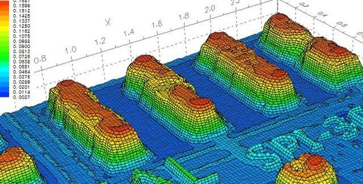
Most solder paste printing machines have the option of including automatic inspection but, depending on the size of the PCB, this process can be time consuming and so a separate machine can often be preferred. The inspection systems within solder paste printers use 2D technology whereas the dedicated SPI machines use 3D technology to enable a more thorough inspection including solder paste volume per pad and not just print area.
Component Placement
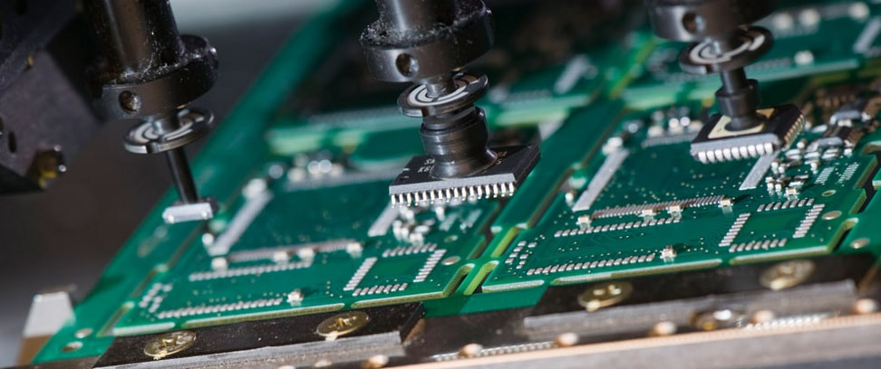
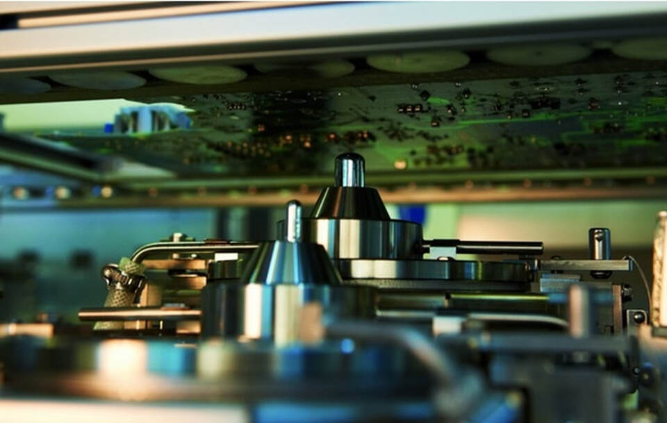
Once the printed PCB has been confirmed to have the correct amount of solder paste applied it moves into the next part of the manufacturing process which is component placement. Each component is picked from its packaging using either a vacuum or gripper nozzle, checked by the vision system and placed in the programed location at high speed.
There is a large variety of machines available for this process and it depends greatly on the business to what type of machine is selected. For example if the business is focused around large build quantities then the placement rate will be important however if the focus is small batch/high mix then flexibility will be more important.
To ensure accurate and repeatable component placement it is important to fully support the PCB being populated - PCB support systems are shown here.
Pre-Reflow Automated Optical Inspection (AOI)
Following the component placement process it is important to verify that no mistakes have been made and that all parts have been correctly placed before reflow soldering. The best way of doing this is by using an AOI machine to make checks such as component presence, type/value and polarity.
First Article Inspection (FAI)
One of the many challenges for sub-contract manufacturers is the verification of the first assembly to the customers information or first article inspection (FAI) as can be very time consuming. This is a very important step in the process as any errors, if undetected, can lead to high volumes of rework.
Reflow Soldering
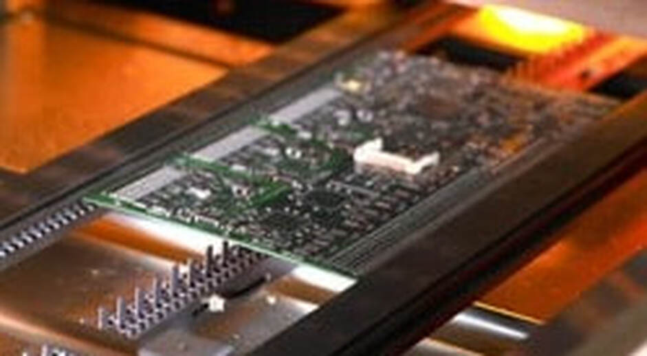
Once all component placements have been checked the PCB assembly moves into the reflow soldering machine where all the electrical solder connections are formed between the components and PCB by heating the assembly to a sufficient temperature. This would appear to be one of the less complicated parts of the assembly processes but the correct reflow profile is key to ensure acceptable solder joints without damaging the parts or assembly due to excessive heat.
When using lead-free solder a carefully profiled assembly is even more important as the required reflow temperature can often be very close to many components maximum rated temperature.
Post-Reflow Automated Optical Inspection (AOI)
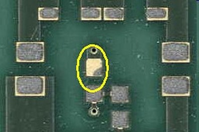
The last part of the surface mount assembly process is to again check that no mistakes have been made by using an AOI machine to check solder joint quality.
With the introduction of 3D technology this process has become more reliable as with 2D inspection there tended to be high levels of false calls due to interpreting a 2D image. 3D inspection has allowed more accurate measurements to be taken and provide a more stable inspection process.
One of the newest features on the inspection machines is that they can be networked together to allow instant feedback to the preceding machine to enable automatic adjustments to be made. For example the AOI machine can be connected to the placement machine so that component placement positions can be adjusted and the SPI machine can be connected to the printer to allow adjustments to be made to the alignment of PCB to stencil.
Through-hole Assembly - Selective Soldering
Although selective soldering is part of the through-hole assembly process, there are many aspects that affect the surface mount assembly and PCB design such as component position.
By designing the PCB with how it will be assembled in mind it is possible to make savings in labour cost and assembly lead time. The first pass yield (FPY) will also be improved by automating as many processes as possible.
Process Verification using X-Ray Inspection
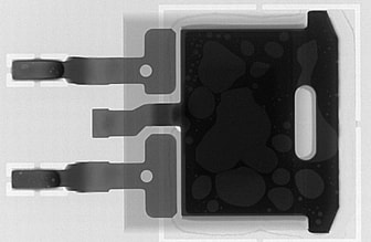
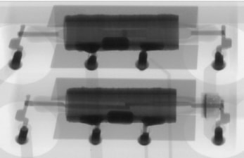
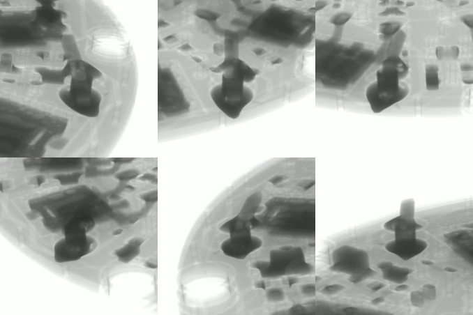
Due to many solder joints being hidden it is important to have a non-destructive method of inspection available that can be used to verify the soldering processes are delivering the desired results.
X-ray inspection provides a way to check underneath components such as BGA's, amount of voiding present within solder joints and also can be used to verify the solder hole fill after soldering process.
X-ray inspection provides a way to check underneath components such as BGA's, amount of voiding present within solder joints and also can be used to verify the solder hole fill after soldering process.
Cleaning 'No-Clean' flux residues and other contaminants
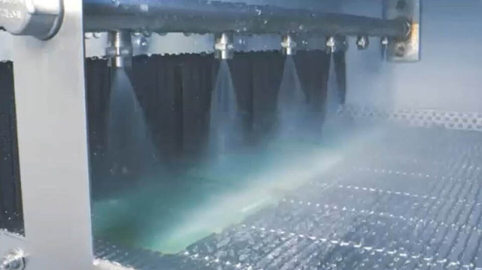
Cleaning is an essential step in the manufacturing process of printed circuit board assemblies to ensure the removal of contaminants, debris, and flux residues that may be left behind after the soldering processes. Although many companies have moved away from using water-soluble fluxes to 'No-Clean', quite often the assemblies still need to be cleaned. Reasons for cleaning include if assembly needs to be conformally coated, if aesthetics are important or if flux residues cause potential current leakage paths in high voltage applications.
Environmental Protection - Conformal Coating
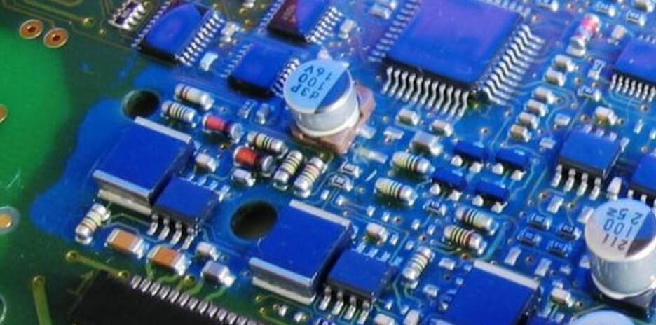
A conformal coating is a thin polymeric film applied to a printed circuit board (PCB) to protect the board and its components from the environment and corrosion. The film is typically applied at 25-250µm and ‘conforms’ to the shape of the board and its components, covering and protecting solder joints, the leads of electronic components, exposed traces, and other metallized areas from corrosion, ultimately extending the working life of the PCB.
Hand Soldering of Surface Mount Components to IPC Class 3
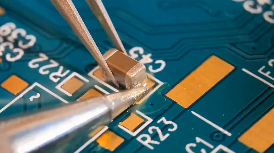
While it is preferable to automatically fit and solder surface mount components, it is sometime necessary to hand fit and solder. This can be a challenge with certain components having very delicate fine-pitch leads, however with specialist knowledge and practice, it is possible.
An Increase in Efficiency and Productivity
It’s a shocking statistic to read that within the electronics industry many surface mount operations, particularly within the sub-contract manufacturing sector, run as low as 20% efficient.
There are many reasons that contribute to this figure but it fundamentally means that only 20% of the capital investment is being utilized. Financially speaking, this will lead to a higher cost of ownership and a slower return on investment. For the customer, it can cause longer lead times for their product and therefore the business will not be as competitive in the market place.
With production efficiencies at this level there will be many knock-on effects that will have an impact on the business such as larger batch sizes, more parts in stock, more assemblies in WIP (work in progress) and slower reaction times to customer change requirements.
With all this in mind there is a strong incentive to improve efficiency while maintaining quality.
We also offer a general consultation service to discuss any particular challenge you may be facing.
If this of interest please send a message using the Contact Page
If this of interest please send a message using the Contact Page
