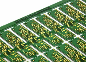
Once the PCB design has been finalized the next phase is to send the PCB data away to a PCB manufacturing company along with a panel design specification to ensure that the format the PCB's are received is as expected.
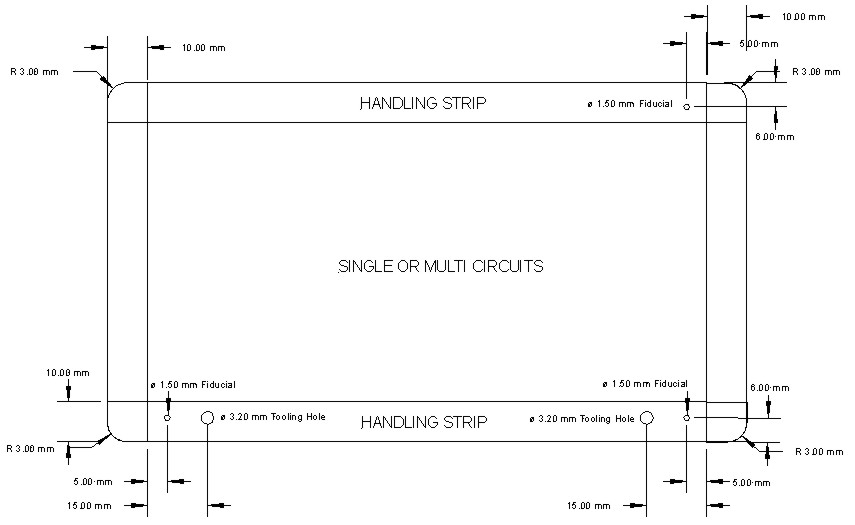
It is recommended that consideration is given to how the bare PCB will be supplied to the PCB assembly company as there needs to be thought given to the machinery that is intended to be used. All the machinery used throughout the process will need ‘tooling strips’ at least on two opposite sides of the panel to allow the PCB to be secured without disturbing the placed components.
As well as the handling consideration it is also important for the following to be considered:-
- Detail the maximum size panel that can be processed by the machinery.
- Adding fiducial marks to allow for the vision alignment systems within the different machines to know exactly where the PCB is to be able carry out the process with a high level of accuracy. The standard practice would be to add three fiducials to the panel in three of the four corners on both sides of the PCB so the machine can determine if the PCB has been loaded incorrectly.
- Adding tooling holes within the handling edges depending if required by the machines that are intended to be used.
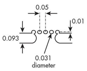
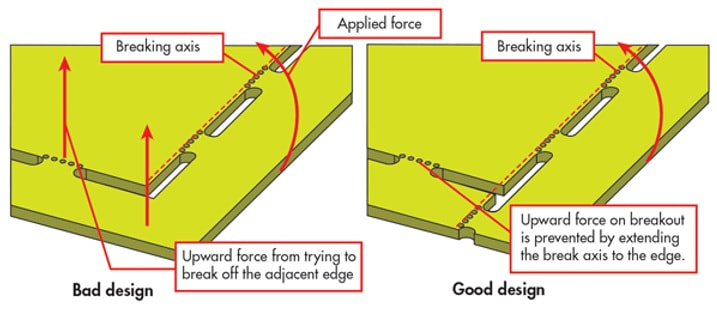
- Method in which the PCB is to be removed from the panel once fully assembled. The usual methods are to either use v-scoring or routing (sometimes a combination of both). If routing is to be used it is important to detail the type of breakouts to be used and also the breakout positions.
- Chain drill the panel waste area to make removing PCB circuit(s) from panel easier after assembly.
- Putting a radius on the panel corners so that when the PCB panels are vacuum packed the panel corners do not break the seal.
- PCB finish - details of the available finishes can be seen here.
Below is an example panel drawing.
Below are details for breakout design if PCB is routed:-
|
Return to home page.
|


