|
|
|
The use of automated optical inspection (AOI) machines is a popular method of inspection, especially in today’s increasing use of microelectronics, and is quickly becoming an integral solution for the surface-mount technology (SMT) industry.
AOI is the automated visual inspection of PCB manufacturing, which uses a camera to scan the assembly for defects that would lead to board failure. It can be used at many stages through the manufacturing process including bare board, solder paste, and populated board inspection (pre- and/or post-reflow). These systems have become more important for manufacturers because they provide incomparable reliability to help maintain high-quality boards with thousands of solder joints and complex and intricate components.
However, does this mean every 3D AOI machine can be the ultimate gatekeeper to identifying defects early in the process? The answer may be both yes and no. Due to increasing component miniaturization, optical inspection systems face many physical limitations, which true 3D-based systems must overcome.
The Path of AOI Inspection
To understand 3D AOI, let’s first look at its predecessor. Introduced in the early 1980s, 2D AOI continues to be one of the most popular forms of inspection today. However, with the “micro” trend increasing and the use of multiple stacked dies in components due to the small footprints being used, the 2D AOI inspection method is not living up to expectations. As technology advances and the world’s insatiable need for the smallest, smartest, and most powerful electronic devices increase, so must production techniques and inspection processes.
Many customers felt that 2D AOI was good enough for their commercial application. However, with the increasing interest in 3D AOI technology and solutions that intelligently combine 2D and 3D technologies to overcome any limitations and provide superior results, the tide is changing.
Many customers felt that 2D AOI was good enough for their commercial application. However, with the increasing interest in 3D AOI technology and solutions that intelligently combine 2D and 3D technologies to overcome any limitations and provide superior results, the tide is changing.
When looking at the path of the optical inspection market, there is clearly a growth. We can see how unsolved difficulties help create innovations. Solder paste inspection (SPI) has undergone a shift from 2D to 3D because 2D technologies that were used to collect a solder deposit image could not solve shadow problems. Several years later, we see the same need for component inspection with AOI systems. As today’s board complexity is increasing with more components and joints, higher density, and new package technologies, 2D AOI technology using grey-scale image analysis or an angled camera view of color images may no longer be a viable option. Most decisions made based on a “good-bad” comparison of reference images can be affected by variables like component surface finish, board condition, component proximity, and more.
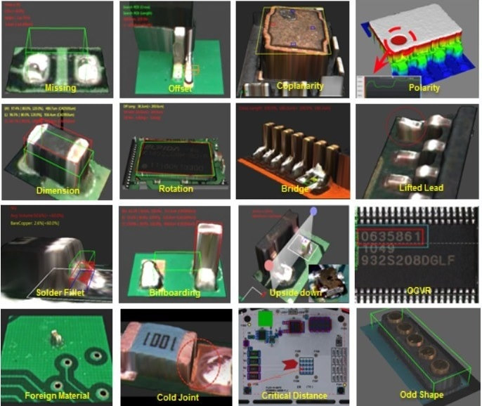
Although 2D AOI is still a major technology in the market, more manufacturers are adopting 3D AOI to increase board quality. 3D AOI improves the measurement accuracy by providing a true measurement of features and detecting aspects like lifted leads or slight changes in coplanarity. This enables the detection of process drift and allows the correction of potential problems before they end up with expensive value-added boards being scrapped.
Although 2D AOI is still a major technology in the market, more manufacturers are adopting 3D AOI to increase board quality. 3D AOI improves the measurement accuracy by providing a true measurement of features and detecting aspects like lifted leads or slight changes in coplanarity. This enables the detection of process drift and allows the correction of potential problems before they end up with expensive value-added boards being scrapped.
Why Choose 3D AOI?
Measurement accuracy is increasingly important within the electronic assembly industry with the decreasing geometry of components, and the need to offer 100% reliable and traceable processes for critical applications. This is especially apparent in the automotive, aerospace, and telecommunications industries, but is becoming increasingly important to most manufacturers as they strive to improve the reliability of electronic assemblies.
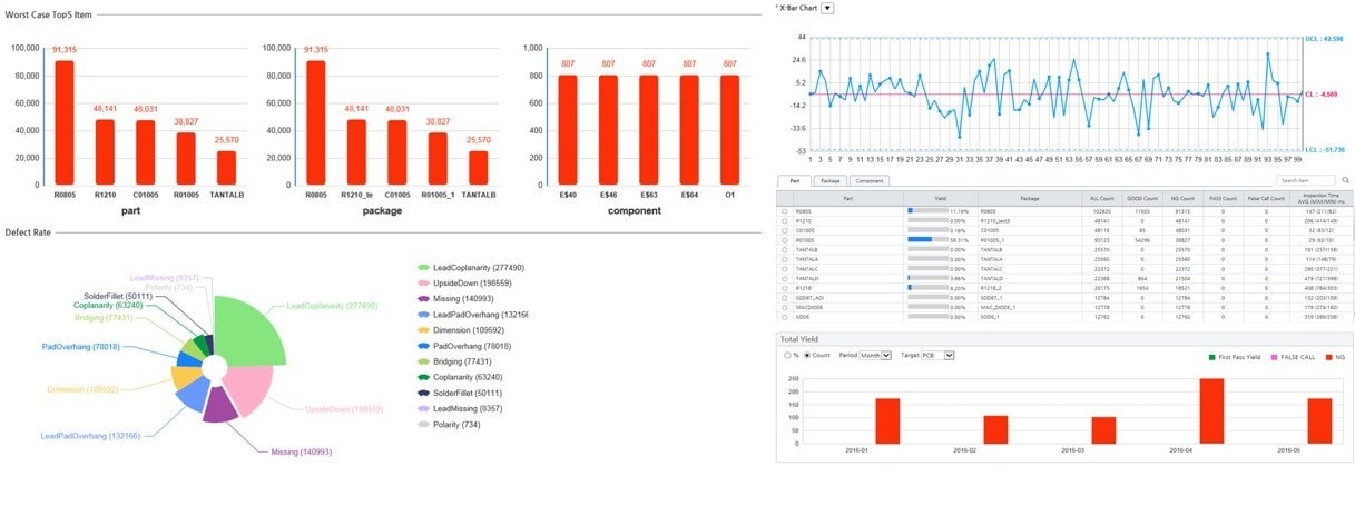
Not only does 3D AOI ensure inspection tolerances are precise, but it also provides meaningful insights about the process that help eliminate the root causes of a defect through measurement data generated from 3D AOIs. The 3D SPI—together with 3D AOI—enables manufacturers to accurately control and monitor the solder printing and component placement processes. It is essential if using 3D AOI equipment to ensure it covers the three “Rs”: reliable, repeatable, and relatable. Another feature to consider is systems that intelligently combine 2D and 3D technologies to offer the best inspection and generate meaningful data, which satisfy the three Rs.
Not only does 3D AOI ensure inspection tolerances are precise, but it also provides meaningful insights about the process that help eliminate the root causes of a defect through measurement data generated from 3D AOIs. The 3D SPI—together with 3D AOI—enables manufacturers to accurately control and monitor the solder printing and component placement processes. It is essential if using 3D AOI equipment to ensure it covers the three “Rs”: reliable, repeatable, and relatable. Another feature to consider is systems that intelligently combine 2D and 3D technologies to offer the best inspection and generate meaningful data, which satisfy the three Rs.
The development of 3D AOI inspection has led to a step change in product quality including greater visibility of problem areas with the ability to measure features, monitor process changes, and take corrective action before the line starts producing failures. Without this, process changes—such as screen print deposition—go unnoticed. Boards are assembled and may pass 2D inspection, but with insufficient solder paste in some areas, the joints may be prone to early life failure. In the worst case, they may pass a functional test and be used in an assembly that ends up in a critical part. For example, the world’s leading car manufacturers do not want ABS modules causing brake failures in the field where recalls and litigation costs could run to millions. These manufacturers will insist on subcontractors making such parts from tried and tested AOI systems that they have qualified after exhaustive testing. Again, the three Rs come into play.
What’s Out There?
When looking for 3D AOI equipment, check its limitations. Some may offer a restricted level of 3D coverage for components and solder joints. Look for innovative systems that provide full 3D coverage to identify boards with defects and monitor performance. Think of the three Rs. Ensure it inspects common defects like missing or wrong components, and accurately identifies coplanarity and lead-bridging issues, which are prevalent in small packages and BGAs.
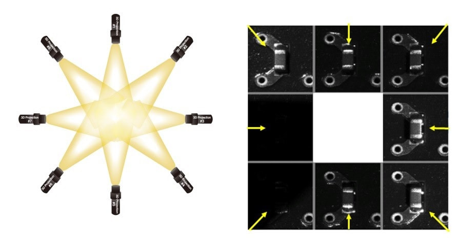
There are systems on the market that measure the Z-axis profilometry of the entire board. By measuring components and solder joints, and then offering critical height information to the inspection algorithms, manufacturers can identify errors like pad overhang and insufficient solder. This results in process optimization, which is difficult to achieve for 2D AOI systems because they do not offer height information. Further, it is impossible to accurately measure and quantify shape, coplanarity, and the solder amount. Unlike 3D AOI systems using a brightness threshold, those that use the height threshold to extract critical body and lead-tip information results in data provide reliable body and joint measurements with CAD dimensions.
Look for systems that combine innovative new technology. Does the 3D AOI system include superior hardware and industry-leading optical technology that generates reliable and repeatable data? Can this data be stored in a central database, which can be used in deploying an optimal program for multiple operations and reducing programming and setting condition times? There is a checklist of features that need to be confirmed before committing to the installation of a 3D AOI system. To ensure your list contains the correct items, it is always best to consult with an expert in the field.
What are the options for post AOI automation?
Whether you are working in an OEM with a fully automated SMT line or in a small subcontractor with island processes, all sites are looking for the next opportunity to maximise their profitability of production.
As with all hardware, how it fits into the process is as important as its capabilities. With no one size fits all, we hope that these options will add value to how you could optimise your automation of post AOI processes. We will discuss, (No Good) Conveyors, NG Workstations, NG Buffers, and multi magazine unloaders.
As with all hardware, how it fits into the process is as important as its capabilities. With no one size fits all, we hope that these options will add value to how you could optimise your automation of post AOI processes. We will discuss, (No Good) Conveyors, NG Workstations, NG Buffers, and multi magazine unloaders.
If you are currently using a batch AOI, then your biggest opportunity for profitability is moving to an inline AOI because you are currently paying a highly-skilled operator to be present 100% of the time it is in use. Sure, a batch system is cheaper at the outset, but not when you consider wages for the person operating it over the machine’s lifetime.
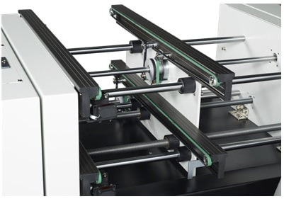
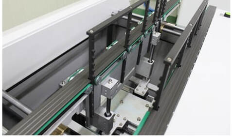
NG Conveyor and NG workstation: Arguably the most common method for post AOI processes and to separate NG PCBAs is the simple yet effective NG Conveyor. These could be 0.5M or 1M and connected via SMEMA/Hermes to the upstream AOI. Fundamentally they have a pin lift mechanism that lifts NG PCBAs from the good transfer conveyor to the NG position above. It can be equipped to up to 3 positions (or 3 NG boards) which then alarms for removal by line operators. These products can then be taken to a review station for processing. This method provides three NG PCBAs worth of automation.
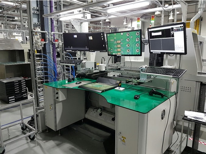
Additionally, to the above, you can create an NG workstation (below) which brings the review station to the SMT line (see below). The fundamental mechanism is the same as a single pin lift, however, the workstation can be equipped with the review station screen and PC and have a mounted optical camera and screen on a floating X, Y gantry so that all the processing and reviews can take place on the line.
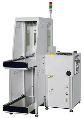
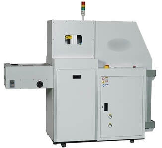
NG Buffer: Another option that is popular in OEM manufacturers as well as CEMs with the ambition of more automation or throughput is the NG Magazine Buffer (as below). In concept, this is a multimagazine unloader that is filled only by NG products post AOI/SPI. This unit offloads perpendicular to the flow of the SMT line and provides the highest level of automation and efficiency as full magazine racks can be taken to the review station and reviewed in bulk for processing. Alarms can be created to reduce unwanted scrap on repetitive consistent faults which will pause production. This option provides 4 magazines worth of automation and for many the equivalent to more than a shift pattern.
Split End of Line Unloader: A great option for those wanting the functionality of the NG Buffer but without the floor space or budget to invest in is a split end of line unloader. With a PLC modification to an unloader immediately downstream from AOI, you can allocate certain magazine positions (say top 5 to NG products which can be variable depending on your NG rate) and the rest to GD products from your AOI. You can then mark on the racks the NG positions which can be separated from GD and sent to review. If there are more NG than slots, the unloader moves to the next empty rack to avoid human error on separation. This option varies in automation depending on the split of NG/GD PCBAS in your production.
Conclusion
As boards become more complex with increasing component miniaturization, the inspection process and how it can be achieved accurately is increasingly important to electronic components longevity. The challenges and limitations of optical inspection systems can no longer be overlooked because they can be the cause for false calls and escapes. While 3D AOI systems are the answer, think twice when suppliers claim 3D inspection; is it modified 2D or full 3D measurement capability? Look for systems that combine technologies with superior hardware to provide true 3D optical inspection solutions and help to guarantee that your inspection process is faultless.
An Increase in Efficiency and Productivity
It’s a shocking statistic to read that within the electronics industry many surface mount operations, particularly within the sub-contract manufacturing sector, run as low as 20% efficient.
There are many reasons that contribute to this figure but it fundamentally means that only 20% of the capital investment is being utilized. Financially speaking, this will lead to a higher cost of ownership and a slower return on investment. For the customer, it can cause longer lead times for their product and therefore the business will not be as competitive in the market place.
With production efficiencies at this level there will be many knock-on effects that will have an impact on the business such as larger batch sizes, more parts in stock, more assemblies in WIP (work in progress) and slower reaction times to customer change requirements.
With all this in mind there is a strong incentive to improve efficiency while maintaining quality.
|
|

