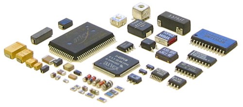
Surface mount component packages are available in wide range of shapes and sizes and are generally designed to be placed by machines rather than by hand.
Passive Two-terminal Components
These components are generally resistors and capacitors and make up the majority of the components placed. Millions are used every day to make the many electronic devices available such as mobile phones and tablets. There are several different sizes available - physical sizes can be seen below:-
|
CLICK HERE FOR CENTROID FILE GENERATION
|
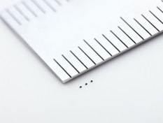 Photo Credit - Murata.com
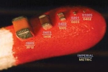
The smallest component seen above on the head of a matchstick is an 01005 (0.4mm x 0.2mm) but there are smaller components currently being placed. These are 008004 parts which measure 0.25mm x 0.125mm and can be seen in the image to the right:-
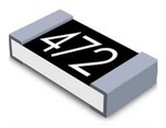
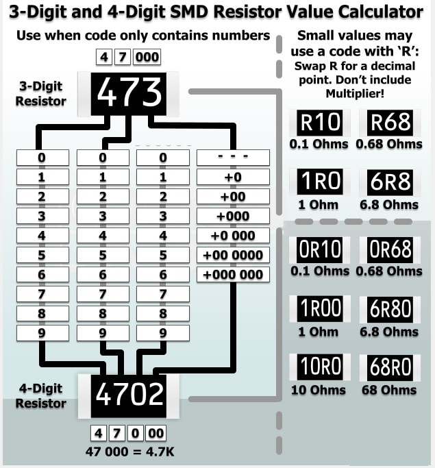
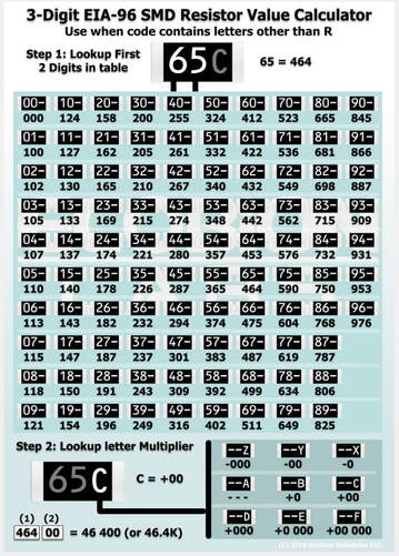
The value of the larger size components can be determined by the code on top of the device - see video and tables below:-
|
|
|
Due to the size of these small components it can be a challenge to see the component itself and an even bigger challenge to read the marking. It is recommended to use either an magnifying glass or a digital microscope that can be seen below:-
|
|
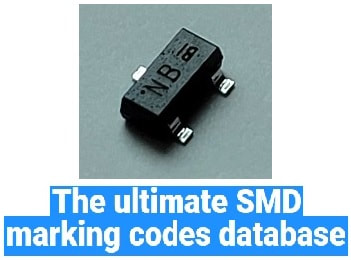
There are many components that are not big enough to fit the complete part number - the example image below shows a SOT-23 device with the code 'NB'.
|
|
In order to correctly identify the component it can be time consuming to find the component datasheet and so the following is a link to - The ultimate SMD marking code database
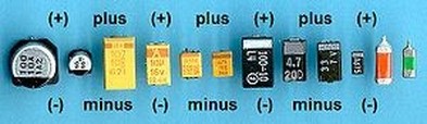
Some passive two-terminal components have a polarity and so it is important for these parts to be fitted in the correct orientation. Some examples of can be seen here:-
Surface Mount Leaded Components
There are different lead styles available but the most common two styles are 'Gull-wing' and 'J-Lead'.
- Gull-wing leads are small and fragile. They can easily be damaged
and must be handled with great care.
- J-leads are more sturdy than gull-wing leads; however, they take up more
space and so there will be fewer leads available on the same size device.
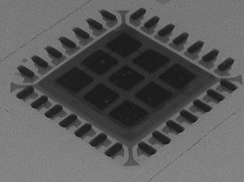
Surface Mount Components without leads
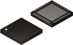
These type of components are usually referred to as 'Bottom Terminated Components' (BTC) and are becoming increasing popular due to their small form factor, reducing cost and good thermal/electrical performance.
One common problem that can occur when soldering these type of devices is voiding. Voiding is simply trapped gas resulting from the soldering process but can cause a reduction in the ability to dissipate heat and may also lift the device leading to open-circuits on the periphery.
A possible solution to reduce the amount of voiding is to change the stencil design for the central ground pad aperture by splitting the aperture to allow space between each solder deposit for the flux outgassing to escape - see below:-
|
|
Reduced voiding under QFN device
|
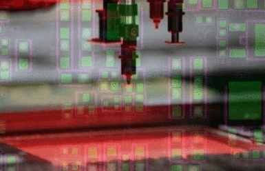
Components with balls! - BGA (Ball-Grid-Array)
A BGA is a type of surface mount device that has been developed to keep up with the demand for the number of electrical connections required for many modern applications. Being sure that these devices are soldered correctly can be a challenge and so process verification is very important.
|
|
|
If PCB space is limited, it is possible to vertically stack IC's - This is known as package-on-package (POP).
|
|
Below is a link to a document that details the terms relating to the many surface mount component packages available:-
| smt_nomenclature.pdf |
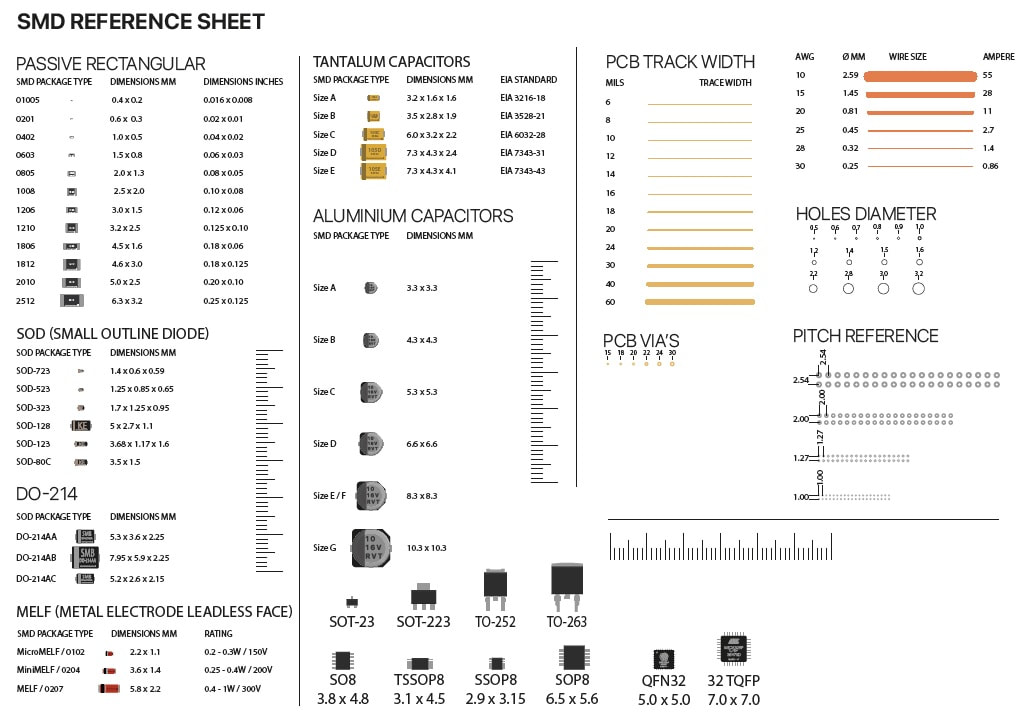
Below is reference sheet for common surface mount packages detailing physical size