So you've got an electronics project that you need to design and need software to make it happen. There are many PCB design tools available online - some which are free and some that come at a cost.
FREE SCHEMATIC, CIRCUIT SIMULATION AND PCB DESIGN TOOLS
- CircuitMaker - Free EDA software tool and a community of creative people, working together to invent circuits and electronics products for a better future.
- PCBWeb - Free CAD application for designing and manufacturing electronics hardware.
- FREEPCB - Free open-source PCB editor for Microsoft Windows, released under the GNU General Public License.
- TinyCAD - Electrical circuit design tool supporting standard and custom symbol libraries.
- ZenitPCB - CAD software for schematic and printed circuit board design.
- OsmondPCB - Planning tool for all those who design circuit boards.
- BSch3V - Basic schematic capture circuit design tool.
- EXPRESSPCB - Schematic capture through to PCB layout.
- KiCAD - Software suite for the creation of professional schematics and printed circuit boards up to 32 copper layers with additional technical layers.
- gplEDA - This electrical circuit design tool runs on Linux and is for circuit and PCB design.
- Fritzing - Open-source PCB design software for electronics projects.
- DESIGNSPARK PCB - Electronics design software, specially designed for rapid prototyping and turning circuit ideas into testable boards.
- EasyEDA - Web and cloud based schematic, circuit simulation and PCB design software.
- XCircuit - Open-source circuit schematic design and simulation software.
- PCB Artist - Basic package is free but many features come at a cost.
- Pad2Pad - Free PCB layout software connected to a REAL circuit board manufacturer.
- PCB123 - Design tool for Printed Circuit Board designers of all levels
PCB DESIGN SOFTWARE AT A COST
- OrCAD - Suite of products for EDA, and includes a schematic editor (Capture), a circuit simulator (PSpice) and a PCB designer.
- CADENCE ALLEGRO - Takes simple or complex designs from concept to production in a constraint-driven design system.
- CADSTAR - Complete design environment for PCB design – from initial concept through to product realization.
- EAGLE - Flexible, expandable and scriptable application with schematic capture editor, PCB layout editor, auto-router and CAM and BOM tools.
- PULSONIX - Choose a combined SCM/PCB product, or Schematic only option.
- EASYPC - Delivering performance in Schematic Capture and PCB Layout normally associated with products at ten or even twenty times the price.
- COMETCAD - circuit schematic and layout editor program for Windows 2k, XP, Vista and 7.
- PADS - The industry-leading, high-productivity, PCB-centric design solution for independent engineers.
- ZUKEN - PCB design software.
- VUTRAX - Electronics schematic and PCB design package.
- MENTOR / VERIBEST - Design Software and Tools offers a comprehensive suite of solutions that improve design, accelerate time to market & increase profit margins.
- ALTIUM DESIGNER - Combines precision, usability, Native 3D, and collaboration to enable engineers and designers to get complex PCB designs done right, the first time.
- DIPTRACE - software for creating schematic diagrams and printed circuit boards.
CAD extraction instructions from the various PCB design software can be seen here.
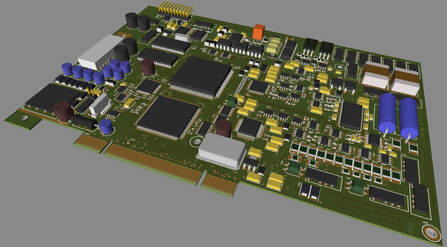
PCB ASSEMBLY DESIGN COMPLETED - PROTOTYPE MANUFACTURE

So you've completed the design for a PCB assembly and need to get some samples made to test. There are an increasing number of companies around the world offering a prototype PCB assembly (PCBA) service such as PCBWay. From reading various reviews the service offered is very good but many require an XY centroid file to be provided along with the Gerber data and Bill of Materials (BOM). Surface Mount Process offer the service to generate the XY centroid file if not available.
