One of the most important parts of the surface mount assembly process is the application of solder paste to the printed circuit board (PCB) – this is generally achieved by the use of a stencil or foil.
A stencil is a thin sheet of material (typically stainless steel) with a series of apertures (holes) cut into it which suit the PCB to be printed.
The function of the solder paste stencil is to accurately deposit the correct amount of solder paste onto the surface mount pads so that the solder joint between PCB pad and component terminal are acceptable with regard to the electrical connection and mechanical strength.
Considerations
The key design features of an effective solder paste stencil are as follows:-
Stencil Thickness
|
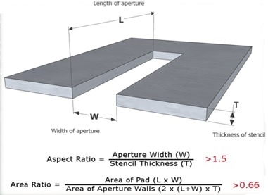
This is important to ensure there is good release of solder paste from the apertures and to obtain the correct volume of solder paste to achieve the desired solder joint. Typically the stencil thickness would be between 4 thou and 8 thou thick. If the stencil is too thick for the size of apertures then it can lead to the paste being held by surface tension to the inner walls of the aperture.
The following is a formula that shows the difference between aspect ratio and area ratio of stencil apertures:-
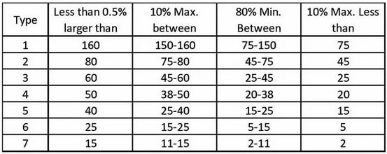
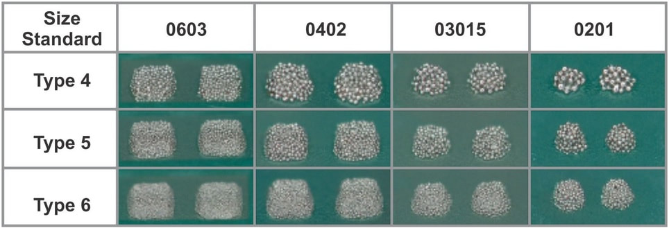
The release of solder paste from the apertures of the stencil is also affected by the particle size of the selected solder paste. Below are the types and particle sizes available:-
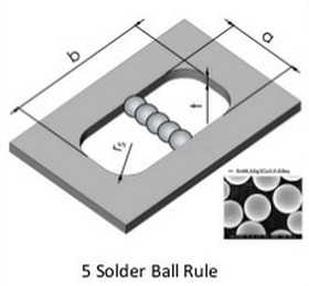
There is a rule of thumb which says ideally a minimum of 5 solder particles should span the width of the smallest aperture.
Aperture Design
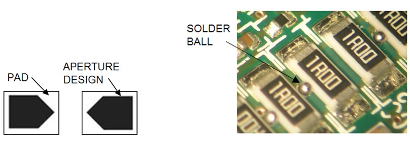
This is important to stop solder defects from forming such as bridging and solder beads. Most apertures are designed to be slightly smaller than the pads (typically 2 thou reduction all round) to provide a good gasket seal between stencil and PCB but some apertures need a special design to deposit less paste on the inner edge of the part to reduce the possibility of ‘mid-chip’ solder balls forming. Below is an example of a possible solution known as ‘home-plate’ apertures and a photo of ‘mid-chip’ solder balls.
|
|
|
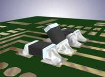
This strategy is effective for components down to 0603 size but when 0402's or smaller are used it can increase the chances of 'tombstoning'. For these smaller size components it is recommended to only have the standard 2 thou reduction or leave 1:1.
There are different aperture shapes within a typical stencil design such as squares, rectangles and circles - all of which have different effects on the transfer of solder paste to the PCB. It may be a surprise to learn but the best aperture shape to achieve the greatest solder paste transfer efficiency is the 'squircle'.
The design of the PCB pads also has a bearing on the resulting solder joints and so it is recommended that IPC standard IPC-7351 is referred to when defining surface mount pad dimensions.
Stencil Material and Mounting
The material type of the stencil will have an impact on its ability to release the solder paste from the apertures. Stainless steel is typically used but for PCB designs that have fine pitch devices a more expensive alternative (Nickel – approx. 50% more expensive than stainless steel) can be used. Other possibilities are to apply a coating to either material to further improve the release of paste from the apertures – An example of this is NanoProTek coating which is an additional fixed cost but does need to be re-applied periodically.
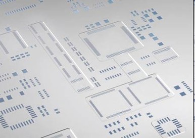
There are occasions where PCB designs contain a large variety of parts including fine pitch devices that require a thin stencil and larger parts that require a thicker stencil. In this case it is possible for a multilevel or ‘stepped’ stencil to be designed. Step-up areas are created by adding material to the stencil and are used to increase the volume and height of the solder paste in selected areas - Useful for ‘pin in paste’ and large format devices. Step-down areas are created by removing material from the stencil and are used to reduce the volume and height of the solder paste deposit in selected areas. In order to print successfully, apertures must be designed to be a minimum distance from the step edge. The distance is dependent on the step dimensions and is known as the ‘keep out area’.
The method in which the stencil is manufactured can affect its ability to release paste from the apertures. The first generation of stencils were chemically etched which provides good results for larger apertures but as the size of components reduced the challenge of solder release from apertures increased. This prompted the introduction of laser-cut stencils which produced a much finer aperture that was trapezoidal in shape and so gave better paste release. Again, as component sizes reduced the option of electro-polishing the aperture walls was introduced and more recently the method of Electro-forming the stencil.
With respect to the stencil mounting, they can be either supplied permanently mounted to a frame or frame-less. The permanently mounted stencils are better suited for high volume printing whereas the frame-less stencils are less expensive and easier to store. The frame-less stencils are designed to work with stencil tensioning systems known as reusable stencil frames – an example being Vectorguard.
Stencil Alignment
In order to achieve an accurate print of the solder paste to the pads, good alignment of the stencil to the PCB is critical. This is achieved by adding registration marks known as fiducial marks to both the PCB and stencil. The addition of fiducial marks to the stencil will ensure good alignment is achieved as shown below.
PCB Design Specific
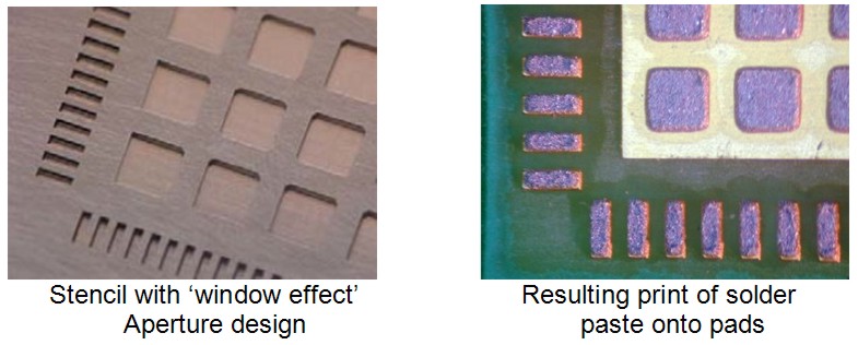
There can be occasions where components within the PCB design have large copper pads underneath the device, which as well as providing a secure electrical connection, are also used to dissipate heat from the device. If the area of the whole pad has solder paste applied it can result in the device lifting and the outer leads not soldering. This can be overcome by creating a ‘window effect’ in the stencil aperture design to reduce the solder volume as can be seen below.
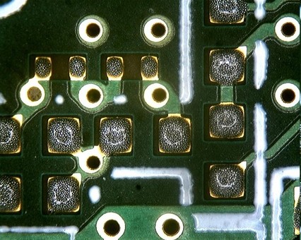
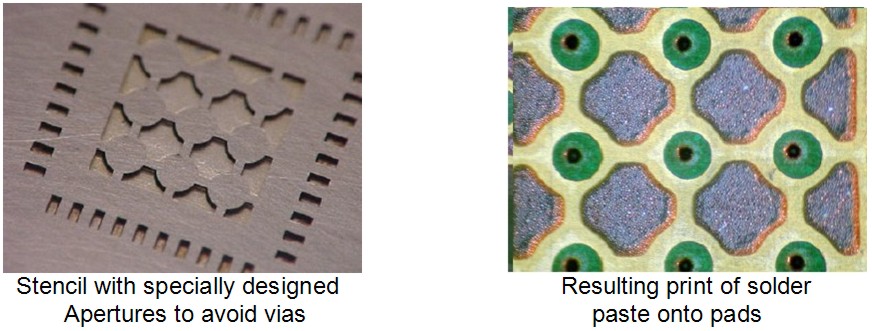
Another PCB design feature on the same type of device that can cause undesirable results is when vias are included within the large copper pad to again dissipate heat from the device. In this case the stencil apertures can be specially designed to avoid the solder paste from being deposited onto the vias as can be seen below.
Conclusion
The printing stage of the assembly process is vitally important. If there are errors introduced at this stage there will be “knock on” effects throughout the process ultimately resulting in process failures. To achieve good repeatable printing results, it is important to use a stencil that is designed with all the appropriate points considered. Most PCB’s can be printed without needing to use a complex stencil design but there can be occasions where it is necessary to use many of the considerations discussed.
An Increase in Efficiency and Productivity
It’s a shocking statistic to read that within the electronics industry many surface mount operations, particularly within the sub-contract manufacturing sector, run as low as 20% efficient.
There are many reasons that contribute to this figure but it fundamentally means that only 20% of the capital investment is being utilized. Financially speaking, this will lead to a higher cost of ownership and a slower return on investment. For the customer, it can cause longer lead times for their product and therefore the business will not be as competitive in the market place.
With production efficiencies at this level there will be many knock-on effects that will have an impact on the business such as larger batch sizes, more parts in stock, more assemblies in WIP (work in progress) and slower reaction times to customer change requirements.
With all this in mind there is a strong incentive to improve efficiency while maintaining quality.
|
|

