|
|
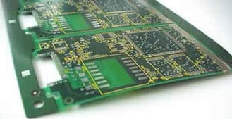
SURFACE MOUNT TROUBLSHOOTING GUIDE
|
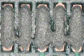
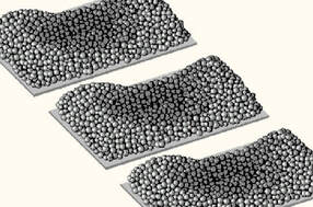
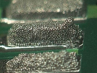
Slump
Causes: Typically due to process being run within an environment outside what is specified within datasheet.
Preventative Actions: Consider installation of temperature control module (TCM) to regulate temperature and humidity within printer. |
|
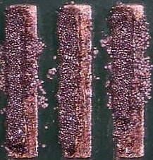
Scooping
Causes: Squeegee pressure set too high, stencil damage, apertures within stencil too large, when using low-temperature lead free paste scooping can be caused by printing too slowly.
Preventative Actions: Divide large stencil apertures. If using low-temperature lead free paste, ensure print speed fast enough. |
|
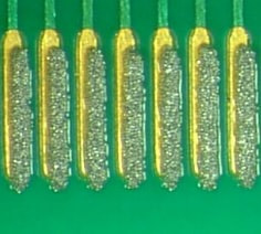
Bridging
Causes: Insufficient PCB support and/or stencil tension, poor stencil condition or cleanliness, poor gasketing between stencil and PCB, solder paste condition, solder paste slump.
Preventative Actions: Check stencil, PCB support & paste |
|
Peaking
Causes: PCB separation (snap off) speed set too high, poor stencil condition or cleanliness, stencil aperature damage.
Preventative Actions: Adjust PCB separation speed, check stencil for damage |
|
Bleeding
Causes: Poor gasketing between PCB and stencil, poor PCB support, squeegee pressure set too high, poor stencil condition or cleanliness.
Preventative Actions: Ensure stencil aperture size is smaller than pads on PCB, improve PCB support, reduce squeegee pressure, check stencil for damage. |
|
Print Misalignment
Causes: Printer alignment error, PCB shrink or stretch, insufficient PCB support.
Preventative Actions: Check alignment of PCB to stencil, ensure fiducial marks are flat and correctly positioned on stencil and PCB. |
|
Partial Print
Causes: Blocked stencil, poor stencil condition or cleanliness, squeegee pressure set too low, solder paste not at room temperature or not fully mixed.
Preventative Actions: Ensure paste fully mixed ideally using automatic mixer, consider using fine-grain material for stencil and/or nano-coating, check aspect ratio. |
|
Excessive Paste affecting small areaCauses: Poor PCB support, damaged stencil, object between PCB and stencil such as a label.
Preventative Actions: Check PCB support - ideally use adaptable system, check stencil for damage, if label has been placed close to affected area relocate. |
|
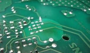
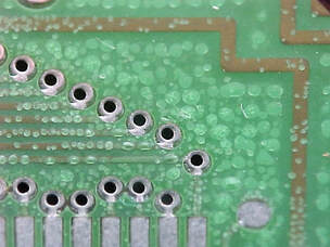
Solder Paste in Through-Holes and Vias
Causes: PCB has been misprinted and not fully cleaned, process for cleaning misprinted PCB is not effective.
Preventative Actions: If PCB is misprinted ensure it is fully cleaned ideally with automatic cleaning process with compatible chemical under pressure to clean all holes. |
|
Centroid File Generation ServiceAt Surface Mount Process we are offering the service to create the component placement file from Gerber data and Bill of Materials. Simply send an enquiry from the contact page
|
Component Placement Defects
|
Solder Paste Pushed Off Pads
Causes: Excessive component placement pressure, faulty component placement sensor on pick and place machine, incorrect component dimensions within package library, PCB not flat due to bow and twist.
Preventative Actions: Set component placement parameters to allow for thickness of solder paste. |
|
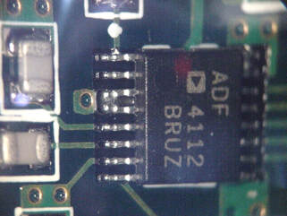
Misaligned Component
Causes: Component disturbed before reflow process, component dropped instead of being placed.
Preventative Actions: Adjust component package parameters within component placement machine library to match dimensions within part datasheet, modify PCB design to ensure all parts are fully visible from above so AOI could detect fault before reflow process. |
|
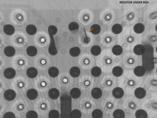
SMD Resistor under BGACauses: SMD resistor dropped on BGA footprint before the BGA component was placed.
Preventative Actions: Check why component dropped (incorrect nozzle, machine fault, machine run too fast), change component placement order to place BGA's first. |
|
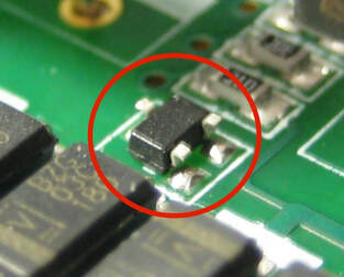
SMD Component Upside Down
Causes: Component flipped over in feeder during index function causing part to be picked and placed upside down.
Preventative Actions: Check indexing function of component feeders is smooth to not cause parts in feeder to flip over. |
|
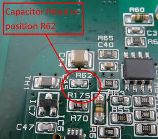
Capacitor fitted in place of Resistor
Causes: Component feeder fitted to incorrect position, when reel of components runs out incorrect reel fitted.
Preventative Actions: Implement machine load check and/or first article inspection (FAI) using smart tweezers, Consider installing electrical test module to component placement machine to detect if incorrect type or value part picked before placement. |
Reflow Soldering Defects
|
Insufficient Solder or Dry Joint
Causes: Via positioned within pad causing solder paste to flow away from pad and through hole during reflow.
Preventative Actions: Modify PCB design to either reposition via outside of component footprint or plug via. |
|
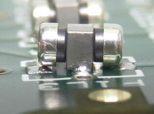
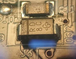
Unsoldered Round SMD Device
Causes: PCB surface finish not flat (HASL), component misplaced, not enough solder paste printed.
Preventative Actions: Consider using flat surface finish such as ENIG, check component parameters in placement machine, ensure enough solder paste printed, increase thickness of solder paste. |
|
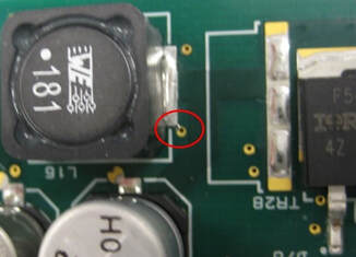
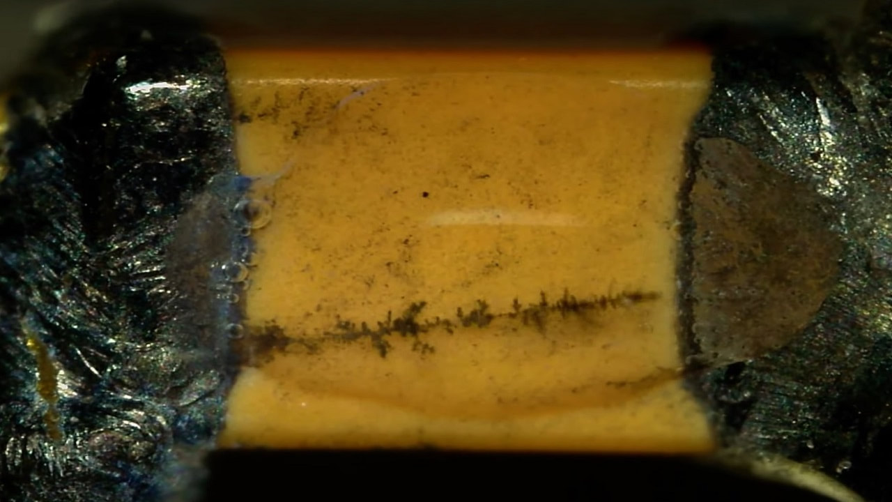
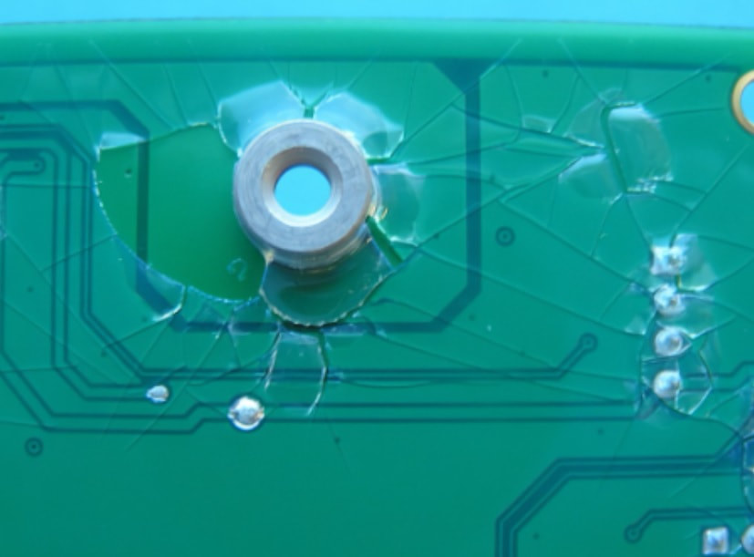
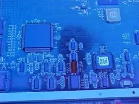
PCB Delamination
Causes: Moisture trapped within FR4 material expanding as PCB is heated by reflow process.
Preventative Actions: Pre-bake PCB's before use and consider using material with higher Tg rating - See here for more details, store PCB's in moisture cabinet. |
|
PCB Measling
Causes: Contamination under solder mask layer, moisture trapped within FR4 material expanding as PCB is heated.
Preventative Actions: Consider alternative PCB supplier, pre-bake PCB's before use and consider using material with higher Tg rating - See here for more details, store PCB's in moisture cabinet. |
|
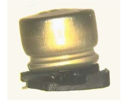
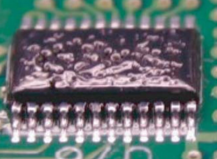
Cracked SMD Capacitor
Causes: Heating rate of reflow profile set too high causing moisture trapped within component to expand as heated by reflow proces.
Preventative Actions: Store components within humidity cabinet or pre-bake before use, reduce heating rate within reflow profile. |
|
Thermally Sensitive Component Damaged
Causes: Incorrect temperature profile during reflow process.
Preventative Actions: Check peak temperature and time above liquidus during reflow. |
|
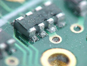
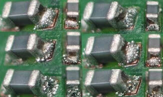
Solder Balls around SMD ComponentsCauses: Heating rate of reflow profile set too high causing flux within solder paste to splatter.
Preventative Actions: Reduce heating rate of reflow profile to no more than 2ºC/second - check solder paste datasheet. |
|
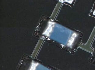
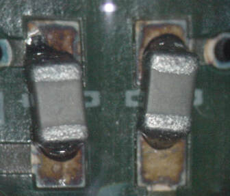
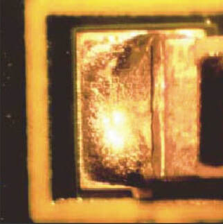
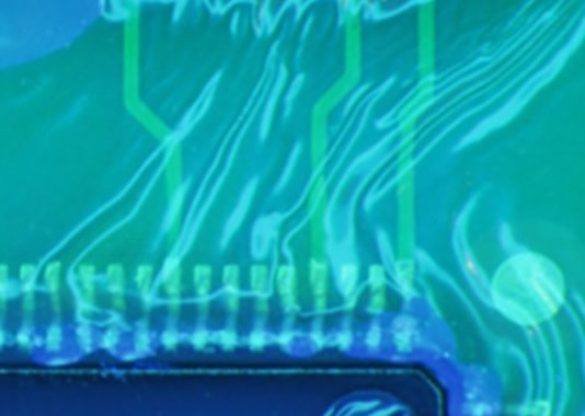
Graping Effect on Solder Joint
Causes: Excessive heat applied during preheat and soak causing flux to become exhausted before entering reflow stage.
Preventative Actions: Reduce time and/or temperature during preheat and soak stage of profile. |
|
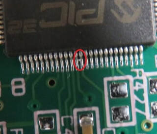
Head-in-Pillow (HIP)
Causes: Excessive heat applied during preheat and soak causing flux to become exhausted before entering reflow stage, oxidised solder connections.
Preventative Actions: Reduce time and/or temperature during preheat and soak stage of profile, consider using nitrogen or higher activity solder paste. |
|
Unconnected BGA Solder JointCauses: Insufficient solder paste applied, poor PCB surface finish, component defect, PCB warped.
Preventative Actions: Check height and volume of paste deposit using 3D SPI before component placement, check PCB solderability, check quality of component, check PCB for bow and twist. |
|
Rough Solder Joint Finish
Causes: Insufficient temperature during reflow stage of profile.
Preventative Actions: Increase temperature and/or time during reflow stage of profile. |
|
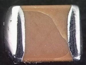
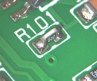
Mid-Chip Solder BallCauses: Incorrect stencil design causing some solder to become separated from the original print during component placement and reflow, incorrect PCB footprint design.
Preventative Actions: Modify stencil aperture design, modify PCB footprint design as per component datasheet. |
|
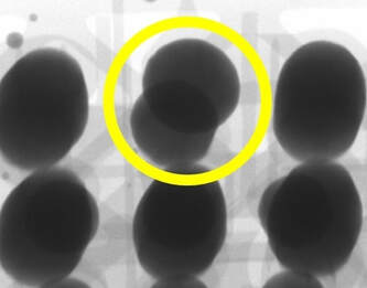
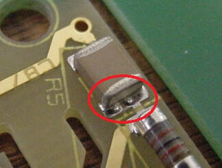
Component Tombstone
Causes: Copper difference either side of component footprint causing thermal imbalance, component misplacement.
Preventative Actions: Modify PCB design to balance copper, modify reflow profile to reduce delta T, improve accuracy of component placement. |
|
Poor PCB Solderability
Causes: Poor PCB quality during manufacture, PCB surface finish deteriorated or damaged during storage.
Preventative Actions: Consider alternative suppliers for PCB's, consider alternative surface finishes, improve method of storage for PCB's. |
|
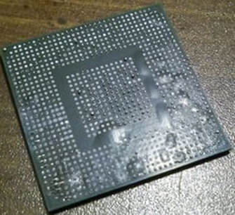
Component Popcorning
Causes: Moisture trapped within component expands as heated by reflow proces.
Preventative Actions: Store components within humidity cabinet or pre-bake before use. |
|
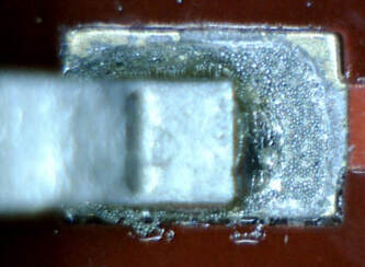
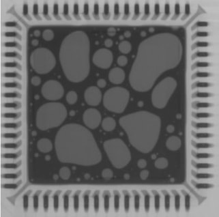
Solder Voiding Underneath Components
Causes: Volatiles released during reflow of solder paste are trapped within solder and not allowed time to escape, vias within pads contributing to gas pockets.
Preventative Actions: Allow more time when solder is molten for volatiles to escape, modify stencil design to allow more pathes for volatiles to escape, consider alternative low-voiding solder pastes, plug vias in PCB. |
|
Component Lifted Lead - Coplanarity
Causes: Component damaged before placement and defect not detected by vision system within component placement machine.
Preventative Actions: Setup coplanarity check within software of component placement machine to detect bent leads. |
|
PCB Bow and Twist
Causes: Defect during PCB manufacturing process, copper imbalance between sides, poor support during reflow.
Preventative Actions: Use copper balancing to even effect of PCB heating and cooling during reflow process, use PCB centre board support during reflow. |
|
No Visible Solder Fillet
Causes: PCB footprint the same size as component so AOI not able to identify solder fillet.
Preventative Actions: Change PCB footprint design using component datasheet or IPC 7351. |
|
Poor Solder Wetting
Causes: Poor component or PCB solderability, poor quality solder paste, incorrect reflow profile.
Preventative Actions: Check PCB and component solderability, check quality of solder paste, check reflow profile to solder paste datasheet. |
|
No Intermetallic Formation
Causes: Poor component solderability, poor quality solder paste, incorrect reflow profile, poor compatibility of PCB finish, solder type, and component termination material.
Preventative Actions: Check PCB and component solderability, check quality of solder paste, check reflow profile to solder paste datasheet. |
|
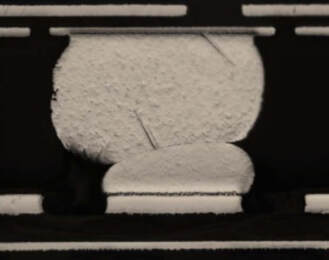
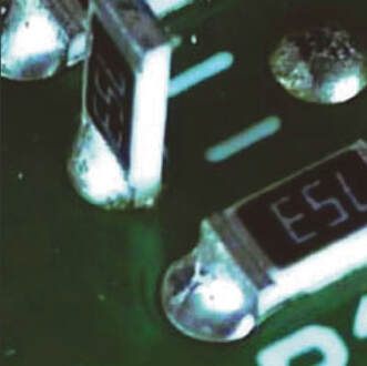
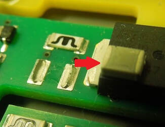
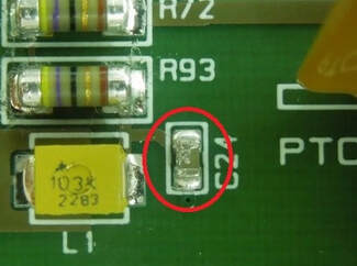
Component Billboard
Causes: Pickup error during component placement process quite often caused by feeder problems.
Preventative Actions: Check feeders on component placement machine are indexing smoothly so parts are not flipped onto their side, adjust vision system on placement machine library to detect parts picked up on their side and reject. |
|
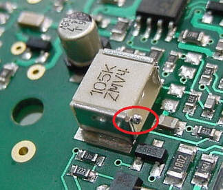
Insufficient or No Solder
Causes: Error during solder paste printing process caused by insufficient solder paste on the stencil or blocked aperture.
Preventative Actions: Ensure enough solder paste is applied to the stencil and is frequently replenished, set printer to clean stencil with appropriate chemical and vacuum, inspect solder paste print before placement. |
|
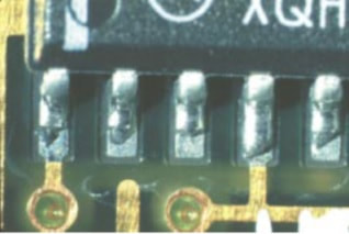
Solder Short on Fine Pitch QFP
Causes: Component misplaced, component disturbed before reflow process, misaligned solder paste print.
Preventative Actions: Check component height, vision parameters and placement speed for component package to ensure accurate placement, ensure good solder paste print using 3D SPI. |
|
Solder Short to Unmasked Via
Causes: PCB unmasked via positioned very close to surface mount component footprint, inaccurate solder paste print.
Preventative Actions: Ideally reposition via further away from component footprint, apply solder mask to via to remove risk of short occurring. |
|
Solder Short due to IC pads being joined
Causes: PCB design had two pads of an IC footprint joined together as electrically were the same point.
Preventative Actions: Recommend changing PCB design to always have separate pads for all component leads even if are electrically connected. |
|
Failure of Rohs Compliant Component
Causes: Rohs compliant component not compatible with reflow process temperature for SAC lead-free solder.
Preventative Actions: Use low temperature lead-free solder, use alternative Rohs compliant component that is compatible with SAC reflow process temperatures. |
|
Solder Joint Cracking
Causes: Poor solderability of component, poor quality solder paste, incorrect reflow profile - incorrect rate of cooling.
Preventative Actions: Check component solderability, check quality of solder paste, check reflow profile to solder paste datasheet. |
|
Solder Short on top of Chip Capacitor
Causes: Solder paste contamination of component during placement process.
Preventative Actions: Discard any misplaced components or ensure cleaned of any solder paste before reuse. |
|
Partial Solder Joint
Causes: Silk print on component footprint pads stopping complete formation of solder joint.
Preventative Actions: Ensure PCB supplier clips away any silk screen from component footprint pads. |
Defects after PCB Cleaning Process
|
Electrochemical Migration (ECM)
Causes: Flux/cleaning chemistry residues and moisture - movement of ions in the presence of an electric field.
Preventative Actions: Ensure all flux/cleaning chemistry residues are fully removed and assembly is completely dry after PCB cleaning process. |
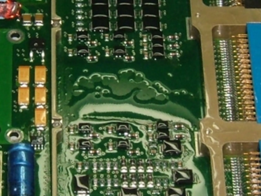
Defects after Conformal Coating Process
|
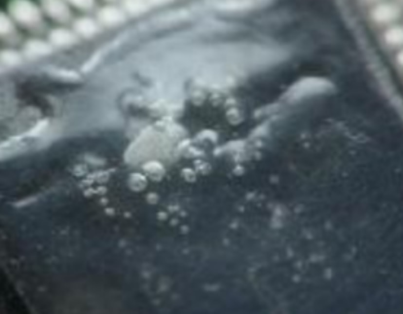
Bubbles
Causes: Improper mixing, high viscosity, contamination, excessive thickness, trapped air, poor application, inadequate drying/curing, too rapid drying/curing, trapped moisture.
Preventative Actions: Ensure conformal coating is mixed correctly, with correct viscosity, free of contamination, is applied from multiple angles, is applied using a controlled method and is dried/cured at the recommended rate. |
|
De-wetting
Causes: Coating incompatibility, poor coating quality, PCB surface contamination.
Preventative Actions: Check the datasheet for chosen coating material to ensure is compatible with PCB material, check coating quality and viscosity, ensure PCB has been cleaned thoroughly and is handled using gloves to avoid finger prints. |
|
Cracking
Causes: Excessive thickness, inadequate drying/curing process, excessive heat during drying/curing.
Preventative Actions: Control thickness during the application process, allow enough time using the correct temperature for coating to dry/cure. |
|
Orange Peel
Causes: Incorrect coating application process, insufficient air pressure during spray application process, incorrect viscosity, incompatible thinner.
Preventative Actions: Check coating application process, air pressure if spray application process used, ensure correct viscosity and regularly check. |
|
Ripples
Causes: Coating too thick, incorrect viscosity, thermal shock due to excessive heat during drying/curing process.
Preventative Actions: Control coating thickness during application process, ensure correct viscosity, implement controlled drying/curing process with appropriate temperature. |
|
Capillary flow
Causes: Excessive coating thickness, low viscosity, varying surface tension across PCB surface being coated.
Preventative Actions: Control coating thickness during application process, ensure correct viscosity, thoroughly clean PCB before coating process. |
|
|
