|
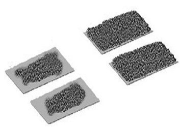
Solder paste partial print, also known as 'incomplete solder paste deposition', is a common defect that can occur during the solder paste printing process. This defect involves the incomplete or insufficient deposition of solder paste onto certain PCB pads or areas, leaving some pads with insufficient solder paste coverage. Solder paste partial print can lead to solder joint defects and negatively impact the functionality and reliability of electronic assemblies.
Causes of Solder Paste Partial Print:
Solder paste partial print can occur due to various factors and process-related issues, including:
- Stencil Aperture Design: The design of the stencil apertures, including their size, shape, and spacing, plays a crucial role in solder paste deposition. Inadequate stencil design may lead to certain areas receiving less solder paste or experiencing inconsistent deposition.
- Stencil Thickness: The thickness of the stencil can affect the amount of solder paste applied. If the stencil is too thick or too thin, it may result in incomplete solder paste printing.
- Squeegee Pressure and Speed: The pressure applied by the squeegee during the solder paste printing process, as well as the speed at which it moves, can affect the consistency of solder paste deposition. Inconsistent pressure or excessive speed may lead to partial prints.
- Solder Paste Viscosity: The viscosity of the solder paste can influence its flow characteristics during the printing process. Solder paste with an inappropriate viscosity may not spread evenly across the stencil apertures, causing partial prints.
- Stencil Cleaning: Residual solder paste on the stencil or in the apertures can lead to variations in paste deposition, contributing to partial prints.
Impact of Solder Paste Partial Print:
Solder paste partial print can have several negative consequences on the SMT assembly process and the quality of electronic assemblies:
- Insufficient Solder Volume: Pads with partial solder paste deposition may not have enough solder to create reliable solder joints, potentially leading to joint defects, poor connectivity, or open circuits.
- Component Misalignment: Incomplete solder paste coverage can lead to misalignment of surface mount components during placement. Components may not align correctly with the pads, affecting solder joint quality.
Preventing and Addressing Solder Paste Partial Print:
To prevent and address solder paste partial print issues in SMT assembly, consider the following strategies:
- Stencil Optimization: Ensure that the stencil design, including aperture size, shape, and spacing, is well-optimized for the components being placed on the PCB. Adequate stencil design can minimize the risk of partial prints.
- Stencil Thickness: Choose an appropriate stencil thickness based on the solder paste type and printing equipment to achieve consistent solder paste deposition.
- Squeegee Control: Control the squeegee pressure and speed to achieve uniform solder paste printing. Proper alignment and calibration of the printing equipment are essential.
- Solder Paste Viscosity: Use solder paste with the appropriate viscosity for your specific application and printing equipment. This can help ensure consistent paste deposition.
- Stencil Cleaning: Maintain proper stencil cleanliness to prevent residual solder paste from interfering with the printing process.
- Solder Paste Inspection (SPI): Implement solder paste inspection equipment to monitor and detect any defects or irregularities in solder paste deposition immediately after printing. SPI can help identify partial print issues in real time.
- Process Optimization: Continuously monitor and optimize the solder paste printing process to minimize the occurrence of partial prints and other defects.
By implementing these strategies and maintaining strict process controls, manufacturers can significantly reduce the risk of solder paste partial print and improve the overall quality and reliability of their electronic assemblies.
