|
|
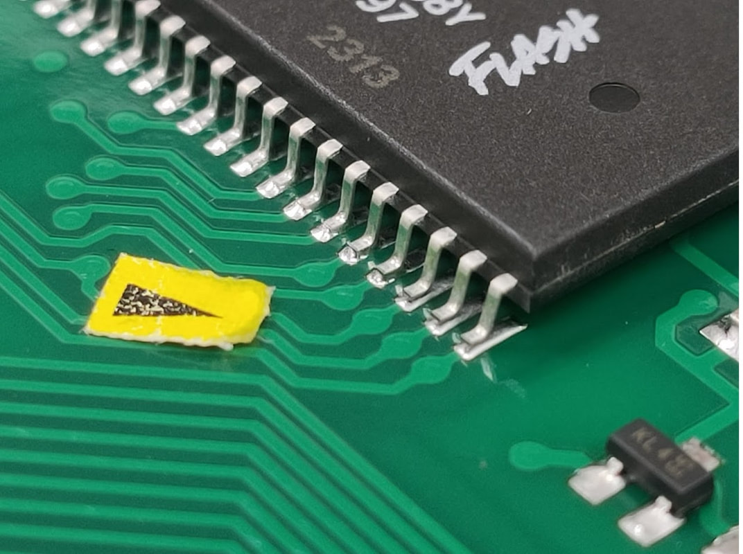
Surface Mount IC component lifted lead or coplanarity issues refer to a situation where the leads or terminals of a surface mount component (SMC) are not flat and not soldered to the PCB pads during reflow soldering. This lack of coplanarity can result in various problems, including poor solder joints, electrical connectivity issues, and mechanical stress on the component. To ensure the coplanarity of SMT component leads, a coplanarity visual check is performed by the component placement machine.
Causes of SMT Component Lifted Lead Coplanarity Fault:
Several factors can contribute to the coplanarity fault during reflow soldering, including:
- Component Handling: Mishandling or excessive force during component placement or reflow can cause leads to become misaligned or lifted.
- Solder Paste Volume: Inadequate or excessive solder paste deposition on PCB pads can lead to uneven solder joint formation.
- Thermal Gradients: Rapid temperature changes during the reflow process can result in differential expansion and contraction rates between the component and the PCB, leading to lifted leads.
- Component Shape and Size: The physical characteristics of the SMT component, such as its body size and lead design, can influence its susceptibility to coplanarity issues.
Impact of SMT Component Lifted Lead Coplanarity Fault:
A coplanarity fault can have several negative consequences on the SMT assembly:
- Solder Joint Reliability: Lifted leads can result in incomplete solder joint formation, leading to poor electrical and mechanical connectivity. These joints may be prone to cracking and failure over time.
- Open Circuits: Depending on the extent of lead misalignment, coplanarity issues can potentially cause electrical open circuits between PCB pads and component leads.
- Mechanical Stress: Coplanarity faults can introduce mechanical stress on the component and the PCB, potentially affecting the assembly's long-term mechanical reliability.
Preventing and Addressing SMT Component Lifted Lead Coplanarity Fault:
To detect and address SMT component lifted lead coplanarity faults, the following steps are typically taken:
- Visual Inspection: Visual inspection is often the initial method used to identify coplanarity issues. Technicians or automated optical inspection (AOI) systems visually inspect components and PCBs for any signs of lead misalignment.
- Measurement Tools: Specialized measurement tools, such as calipers, vision systems, or 3D scanning devices, may be employed to quantify the extent of the coplanarity fault.
- Acceptance Criteria: Manufacturers define acceptable coplanarity limits based on industry standards or internal quality control standards. Components that exceed these limits may require corrective action.
- Remediation: Corrective actions may involve reflowing the solder joints, replacing the component with one that meets coplanarity requirements, or adjusting the assembly process parameters.
- Process Improvement: Manufacturers may implement process improvements, such as optimizing the reflow profile, enhancing component placement accuracy, and refining solder paste deposition techniques, to prevent coplanarity faults in future assemblies.
Addressing coplanarity faults during reflow soldering is essential to ensure the reliability and functionality of electronic assemblies. Early detection and appropriate corrective measures are key to mitigating the negative effects of this common SMT assembly issue.
