|
|
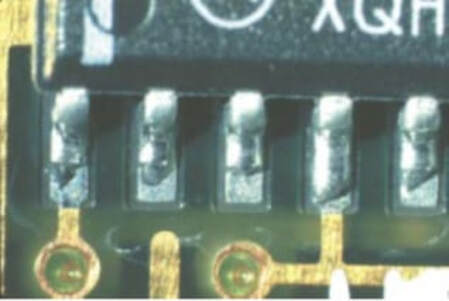
Poor solder wetting in surface mount soldering refers to an undesirable condition in which the molten solder does not adequately flow and adhere to the surfaces it is supposed to bond during the soldering process. Proper solder wetting is essential for creating reliable and robust solder joints in surface mount technology (SMT) assembly. When wetting is poor, several issues can arise, potentially leading to solder joint defects and overall assembly reliability problems.
Causes of Poor Solder Wetting:
- Contamination: Contaminants such as oxide layers, dust, or residue on the solderable surfaces (e.g., component leads or PCB pads) can prevent proper wetting. Solder has difficulty displacing these contaminants, leading to poor adhesion.
- Incorrect Solder Alloy: The choice of solder alloy and flux may not be suitable for the specific components and PCB materials, resulting in poor wetting properties.
- Improper Solder Paste: Inconsistent or incorrect application of solder paste, including insufficient or excessive deposition, can lead to poor wetting during reflow soldering.
- Insufficient Preheating: Inadequate preheating of the assembly before reflow can prevent the solder from flowing properly. Preheating helps reduce thermal shock and enables better wetting.
- Inadequate Soldering Temperature: Soldering below the recommended temperature range for the specific solder alloy can hinder proper wetting. The solder may not become sufficiently fluid to bond effectively.
- Component Misalignment: If surface mount components are not accurately placed on the PCB pads, the solder may not make proper contact with both the component lead and the pad, resulting in poor wetting.
Consequences of Poor Solder Wetting:
- Incomplete Solder Joints: Poor solder wetting can lead to incomplete solder joints where the solder does not fully cover the component lead and the pad. This can result in poor electrical and mechanical connections.
- Solder Bridges: Inadequate wetting can cause adjacent solder joints to merge, leading to solder bridges or short circuits between conductive elements on the PCB.
- Solder Balls: Excess solder may not wet properly and may form spherical blobs or "solder balls" on the PCB surface, potentially causing short circuits and contamination.
- Reliability Issues: Solder joints with poor wetting are prone to mechanical stress, thermal cycling, and potential failure over time, reducing the overall reliability of the assembly.
To address poor solder wetting in surface mount soldering, manufacturers should take steps to:
By addressing the root causes of poor solder wetting and implementing best practices in SMT assembly processes, manufacturers can achieve high-quality, reliable solder joints and assemblies.
- Ensure proper cleaning and preparation of component leads and PCB pads.
- Select appropriate solder alloys and fluxes for the application.
- Optimize solder paste deposition techniques, stencil design, and reflow profiles.
- Implement accurate component placement and use inspection techniques to verify alignment.
- Monitor and control process parameters, including temperature and atmosphere, to ensure optimal wetting conditions.
By addressing the root causes of poor solder wetting and implementing best practices in SMT assembly processes, manufacturers can achieve high-quality, reliable solder joints and assemblies.
