|
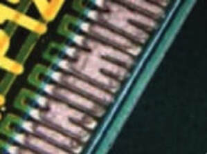
Solder paste bridging, also known as "solder shorting," is a common defect that can occur during the surface mount technology (SMT) soldering process, specifically during reflow soldering. It involves the unintended connection or short circuit between adjacent solder joints, typically between closely spaced surface mount components or component leads. Solder bridging can have negative consequences on the functionality and reliability of electronic assemblies, and it is essential to prevent and address this issue in SMT assembly processes.
Causes of Solder Paste Bridging:
Solder paste bridging can result from a variety of factors and process-related issues, including:
- Stencil Aperture Design: The design of the stencil apertures, including their size, shape, and spacing, can significantly influence the likelihood of bridging. Apertures that are too close together or inadequately sized are more prone to solder paste bridging.
- Stencil cleanliness: During solder paste printing process, the solder paste can come into contact with stencil underside and smudge. Under-stencil cleaning should be regularly (automatically or manually) carried out to maintain print quality.
- PCB Support: If PCB's are not fully supported, excessive solder paste can be deposited onto the PCB's - this will provide high risk of bridging, especially with fine-pitch components.
- Solder Paste Printing: Inconsistent or excessive solder paste deposition during the printing process can lead to bridging. Factors such as stencil alignment, squeegee pressure, and solder paste viscosity can affect the amount of paste applied.
- Component Placement: The accuracy and precision of component placement on the PCB are crucial. Misaligned or improperly positioned components increase the risk of bridging between component leads.
- Reflow Profile: The reflow soldering temperature profile, including the preheat, soak, and reflow phases, must be carefully controlled. An inappropriate temperature profile can cause premature melting of solder paste and bridging.
- Solder Alloy and Flux: The composition of the solder alloy and the type of flux used can influence solder paste flow and wetting characteristics. Incompatible solder paste and flux formulations may lead to bridging.
Impact of Solder Paste Bridging:
Solder paste bridging can have several negative consequences on the SMT assembly process and the quality of electronic assemblies:
- Electrical Shorts: Solder bridging creates unintended electrical connections between components or component leads, potentially causing circuit malfunctions or damage to sensitive components.
- Mechanical Stress: Bridging can result in increased mechanical stress on solder joints, potentially leading to joint failure or reduced reliability.
- Rework and Repair: Detecting and correcting solder bridging often requires rework or repair, which can increase production costs and assembly time.
Preventing and Addressing Solder Paste Bridging:
To prevent and address solder paste bridging issues in SMT assembly, consider the following strategies:
- Stencil Optimization: Ensure that the stencil design, including aperture size, shape, and spacing, is well-optimized for the components being placed on the PCB to minimize the risk of bridging.
- Stencil Cleaning: Keep the stencil clean and free from residual solder paste to ensure consistent paste deposition.
- PCB Support: If PCB's are large and/or thin, they will need support to enable a good and repeatable solder paste print. This can be a challenge for double sided assemblies.
- Component Placement: Implement precise and accurate component placement techniques to minimize the risk of misaligned components and bridging. Component placement pressure is an important factor as if set too high can cause displacement of solder paste from PCB pads.
- Solder Paste Inspection (SPI): Use solder paste inspection equipment to monitor and detect any defects or irregularities in solder paste deposition immediately after printing. SPI can help identify and address bridging issues in real time.
- Reflow Profile Control: Maintain proper control of the reflow soldering temperature profile to ensure that solder paste melts and reflows correctly without causing bridging.
- Solder Alloy and Flux Compatibility: Ensure that the solder paste and flux formulations are compatible and well-suited for the specific SMT assembly process.
- Process Optimization: Continuously monitor and optimize the solder paste printing and reflow soldering processes to minimize the occurrence of bridging and other defects.
By implementing these strategies and maintaining strict process controls, manufacturers can significantly reduce the risk of solder paste bridging and improve the overall quality and reliability of their electronic assemblies.
