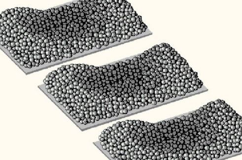
Solder paste scooping is a common issue that can occur during the surface mount technology (SMT) assembly process, particularly when applying solder paste to printed circuit boards (PCBs) using a stencil. It refers to the unintended separation or gap in the deposited solder paste, resulting in an incomplete or disconnected solder joint. Solder paste scooping can lead to poor solder joint quality and negatively affect the functionality and reliability of electronic assemblies.
Causes of Solder Paste Scooping:
Solder paste scooping can occur due to several factors and process-related issues:
- Stencil Design: The design of the solder paste stencil, including aperture size, shape, and spacing, can significantly influence the likelihood of scooping. Inadequate stencil design may lead to misalignment of apertures or the formation of irregular shapes.
- Stencil Thickness: The thickness of the stencil can impact the amount of solder paste deposited. If the stencil is too thick, it may result in insufficient solder paste being applied, increasing the risk of scooping.
- Squeegee Pressure and Speed: The pressure applied by the squeegee during the solder paste printing process, as well as the speed at which it moves, can affect the consistency of solder paste deposition. Inconsistent pressure or excessive speed may cause scooping.
- Solder Paste Viscosity: The viscosity of the solder paste can influence its flow characteristics. Solder paste with an inappropriate viscosity may not spread evenly across the stencil apertures, leading to scooping.
- Solder Paste Consistency: Inconsistent solder paste consistency within the container can result in non-uniform deposition and scooping. It's important to properly mix and store solder paste to maintain its homogeneity.
Impact of Solder Paste Scooping:
Solder paste scooping can have various negative consequences on the SMT assembly process and the quality of electronic assemblies:
- Incomplete Solder Joints: Scooping can result in incomplete solder joints or solder joints with gaps, reducing their mechanical strength and electrical conductivity.
- Solder Bridging: In some cases, solder paste that is displaced by scooping can bridge adjacent pads or leads, leading to solder bridging defects.
Preventing and Managing Solder Paste Scooping:
To prevent or address solder paste scooping issues in SMT assembly, consider the following strategies:
- Stencil Optimization: Ensure that the stencil design, including aperture size, shape, and spacing, is well-optimized for the components being placed on the PCB.
- Stencil Thickness: Choose an appropriate stencil thickness based on the solder paste type and printing equipment to achieve consistent solder paste deposition.
- Squeegee Control: Control the squeegee pressure and speed to achieve uniform solder paste printing. Maintain proper alignment and calibration of the printing equipment.
- Solder Paste Quality: Use high-quality solder paste with consistent viscosity and homogeneity. Properly store and handle solder paste to prevent variations in consistency.
- Solder Paste Inspection: Implement solder paste inspection (SPI) equipment to monitor and detect any irregularities in solder paste deposition immediately after printing. This can help identify and address scooping issues in real time.
- Process Optimization: Continuously monitor and optimize the solder paste printing process to minimize the occurrence of scooping and other defects.
Solder paste scooping is a common challenge in SMT assembly, but with proper process control, stencil design, and equipment maintenance, it can be managed to ensure the reliability and quality of solder joints in electronic assemblies.

