SURFACE MOUNT PROCESS
  • Home
  • Articles
    • A GUIDE TO EFFECTIVE STENCIL DESIGN
    • SOLDER PASTE PRINTING PROCESS
    • SOLDER PASTE INSPECTION PROCESS
    • COMPONENT PLACEMENT PROCESS
    • REFLOW SOLDERING PROCESS
    • POST-REFLOW AOI PROCESS
    • THROUGH-HOLE ASSEMBLY - SELECTIVE SOLDERING
    • Cleaning 'No-Clean' flux residues and other contaminants
    • Environmental Protection - Conformal Coating
    • Hand soldering and rework of surface mount components to IPC class 3
  • FAQ
    • Solder paste handling
    • Type 3 or Type 4 Solder Paste
    • Cleaning a misprinted PCB
    • Solder Paste Quality Control
    • What factors affect solder paste transfer efficiency
    • What stencil thickness should be used?
    • What is the difference between aspect ratio and area ratio of stencil apertures?
    • What squeegee speed should be used?
    • What squeegee pressure should be used?
    • What the differences between 'on-contact' printing and 'gap' printing?
    • What separation speed to use in solder paste printing?
    • What are the benefits / challenges of using halogen-free solder paste?
    • What is the best stencil aperture shape for solder paste transfer efficiency?
    • PCB delamination during reflow
    • What are the different types of reflow profile?
    • ROSE (Resistivity of Solvent Extract) testing
    • How do you validate a PCBA cleaning process?
    • Why clean a pcba that has been soldered using no-clean flux
    • How do engineered cleaning fluids such as Zestron and Kyzen work
    • How do engineered cleaning fluids affect surface tension and wetting angle?
    • How does the pH level affect engineered cleaning fluids?
    • How do mixed-bed and carbon filters work in PCB cleaning systems?
    • What are the risks of using ultrasonics to clean PCBA's?
    • What are the differences between 'Water-soluble' and 'No-clean' flux?
    • What is the difference between ionic and non-ionic contamination?
    • What causes electrochemical migration (ECM)?
    • What are methods of masking before conformal coating?
    • How to apply conformal coating by brushing?
    • How to apply conformal coating using dipping?
    • How to apply conformal coating using spray/aerosol?
    • How do selective robots apply conformal coating?
    • What is the best method to dry/cure conformal coating?
    • What concerns are there when demasking?
    • What should be checked when inspecting after conformal coating?
    • How to check the adhesion of conformal coating?
    • Tape and Reel Packaging Standards
    • What is 'Package on Package' (POP)?
    • Stock control and component attrition
    • BOM Comparison Software
    • Comparison of SAC305 and SAC387 Lead-Free Solder Alloys
    • What is a 'Eutectic' solder alloy?
    • What does 'SMT' stand for?
    • What does the term voiding mean?
    • How is void percentage calculated?
    • How to reduce voids in QFN device ground connection?
    • Low temperature lead free solder paste
    • CAD EXTRACTION
    • How are PCB's manufactured?
    • What are the IPC standards that govern electronics manufacturing processes?
    • What are the differences between SMEMA and HERMES?
  • Contact
  • Store

Solder Paste Slump - Printing Defect

Picture
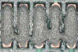
Solder paste slump is a phenomenon that can occur in the process of applying solder paste to printed circuit boards (PCBs) during surface mount technology (SMT) assembly. It refers to the deformation or settling of the solder paste after it has been applied but before the components are placed and the PCB is subjected to reflow soldering. Solder paste is a crucial material in SMT assembly, and its proper placement is essential for reliable solder joints. Here's a more detailed explanation of solder paste slump:

Causes of Solder Paste Slump:

Solder paste slump can occur due to several reasons, including:

  1. Gravity: Solder paste is a dense, viscous material. When it is applied to the PCB, it may begin to flow or sag under the influence of gravity.
  2. Temperature: Temperature variations in the assembly environment can affect the viscosity of the solder paste. If the environment is warmer, the solder paste may become less viscous and more prone to slump.
  3. Time Delay: If there is a significant time delay between applying the solder paste and placing the components on the PCB, the paste may have more time to settle and deform.
  4. Stencil Design: The design of the solder paste stencil, including aperture size and shape, can influence the amount of paste applied and its tendency to slump.

Impact of Solder Paste Slump:

Solder paste slump can have several negative consequences in the SMT assembly process:

  1. Solder Short/Bridge: A solder bridge is common result of slumped solder after reflow.
  2. Component Misalignment: Slumped solder paste can lead to misalignment of SMT components during placement. This can result in components being positioned incorrectly, affecting the functionality and reliability of the PCB.
  3. Uneven Solder Joints: If the solder paste has settled unevenly, it can lead to uneven solder joint formation during reflow soldering. This can result in solder joint defects, including insufficient solder volume or solder bridging.

Preventing and Managing Solder Paste Slump:

To prevent or mitigate solder paste slump, consider the following strategies:

  1. Optimize Solder Paste Viscosity: Choose a solder paste formulation with the appropriate viscosity for your specific application and environmental conditions.
  2. Stencil Design: Ensure that the solder paste stencil design, including aperture size and spacing, is optimized for the components being placed on the PCB.
  3. Timely Component Placement: Minimize the time delay between solder paste application and component placement. Some automated SMT equipment can minimize this delay.
  4. Stabilize Environmental Conditions: Maintain a stable temperature and humidity environment in the assembly area to minimize variations in solder paste viscosity.
  5. Use Solder Paste Inspection: Implement solder paste inspection (SPI) equipment to monitor and detect any irregularities in solder paste deposition immediately after printing. This can help identify and address slump issues in real time.

Solder paste slump is a common challenge in SMT assembly, but with proper process control, stencil design, and equipment, it can be managed to ensure the reliability of solder joints and the overall quality of electronic assemblies.
© COPYRIGHT 2015. ALL RIGHTS RESERVED.