SURFACE MOUNT PROCESS
  • Home
  • Articles
    • A GUIDE TO EFFECTIVE STENCIL DESIGN
    • SOLDER PASTE PRINTING PROCESS
    • SOLDER PASTE INSPECTION PROCESS
    • COMPONENT PLACEMENT PROCESS
    • REFLOW SOLDERING PROCESS
    • POST-REFLOW AOI PROCESS
    • THROUGH-HOLE ASSEMBLY - SELECTIVE SOLDERING
    • Cleaning 'No-Clean' flux residues and other contaminants
    • Environmental Protection - Conformal Coating
    • Hand soldering and rework of surface mount components to IPC class 3
  • FAQ
    • Solder paste handling
    • Type 3 or Type 4 Solder Paste
    • Cleaning a misprinted PCB
    • Solder Paste Quality Control
    • What factors affect solder paste transfer efficiency
    • What stencil thickness should be used?
    • What is the difference between aspect ratio and area ratio of stencil apertures?
    • What squeegee speed should be used?
    • What squeegee pressure should be used?
    • What the differences between 'on-contact' printing and 'gap' printing?
    • What separation speed to use in solder paste printing?
    • What are the benefits / challenges of using halogen-free solder paste?
    • What is the best stencil aperture shape for solder paste transfer efficiency?
    • PCB delamination during reflow
    • What are the different types of reflow profile?
    • ROSE (Resistivity of Solvent Extract) testing
    • How do you validate a PCBA cleaning process?
    • Why clean a pcba that has been soldered using no-clean flux
    • How do engineered cleaning fluids such as Zestron and Kyzen work
    • How do engineered cleaning fluids affect surface tension and wetting angle?
    • How does the pH level affect engineered cleaning fluids?
    • How do mixed-bed and carbon filters work in PCB cleaning systems?
    • What are the risks of using ultrasonics to clean PCBA's?
    • What are the differences between 'Water-soluble' and 'No-clean' flux?
    • What is the difference between ionic and non-ionic contamination?
    • What causes electrochemical migration (ECM)?
    • What are methods of masking before conformal coating?
    • How to apply conformal coating by brushing?
    • How to apply conformal coating using dipping?
    • How to apply conformal coating using spray/aerosol?
    • How do selective robots apply conformal coating?
    • What is the best method to dry/cure conformal coating?
    • What concerns are there when demasking?
    • What should be checked when inspecting after conformal coating?
    • How to check the adhesion of conformal coating?
    • Tape and Reel Packaging Standards
    • What is 'Package on Package' (POP)?
    • Stock control and component attrition
    • BOM Comparison Software
    • Comparison of SAC305 and SAC387 Lead-Free Solder Alloys
    • What is a 'Eutectic' solder alloy?
    • What does 'SMT' stand for?
    • What does the term voiding mean?
    • How is void percentage calculated?
    • How to reduce voids in QFN device ground connection?
    • Low temperature lead free solder paste
    • CAD EXTRACTION
    • How are PCB's manufactured?
    • What are the IPC standards that govern electronics manufacturing processes?
    • What are the differences between SMEMA and HERMES?
  • Contact
  • Store

What causes electrochemical migration (ECM)?

Electrochemical migration (ECM) is primarily caused by the movement of ions in the presence of an electric field. ECM occurs in electronic circuits, particularly on printed circuit boards (PCBs), and can lead to the formation of unintended electrical paths and electrical shorts. Several factors contribute to the occurrence of ECM:

  1. Voltage Bias: ECM typically occurs when a voltage bias is applied to a PCB or electronic circuit. This bias can be the result of power supply voltages, signals, or other electrical potentials within the circuit.
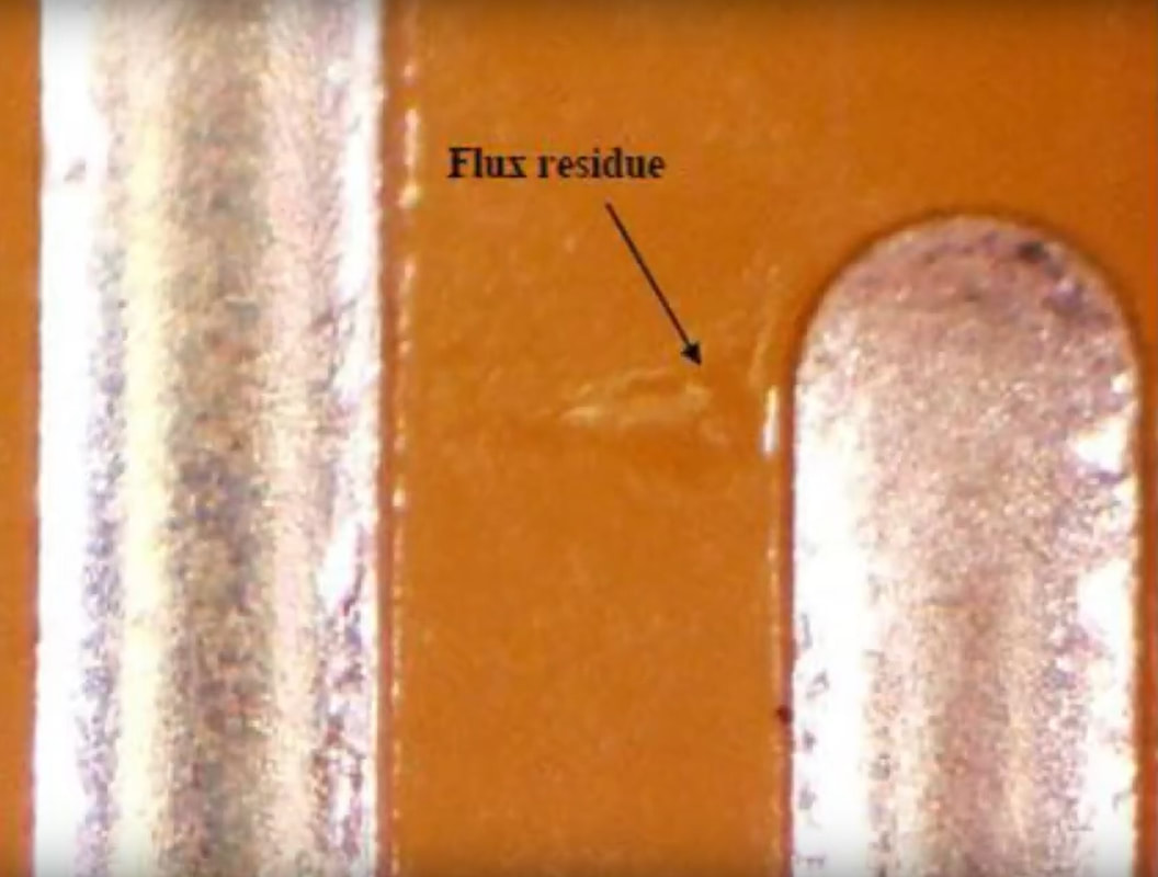
  2. Ionic Contaminants: The presence of ionic contaminants on the PCB or within its environment is a key factor in ECM. These contaminants consist of ions such as sodium (Na+), chloride (Cl-), and others. Contaminants can be introduced during the manufacturing process or as a result of environmental exposure.
  3. Electric Field: The application of a voltage bias creates an electric field within the electronic circuit. This electric field exerts a force on the ionic contaminants, causing them to move.
  4. Ion Migration: Under the influence of the electric field, ionic contaminants can migrate, moving along the surface or within the PCB substrate. The movement of ions is driven by the attraction of ions of opposite charges towards the electrodes of the bias.
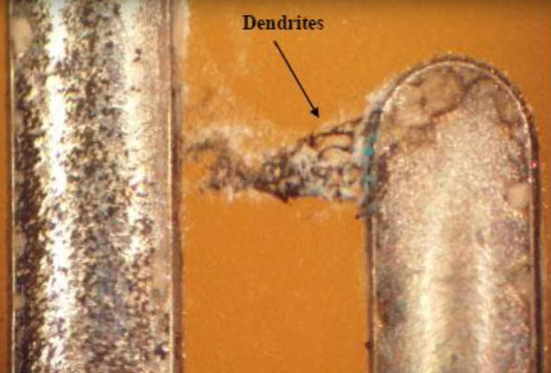
  5. Path Formation: As the ions move, they can create unintended electrical paths or bridges (dendrite or dendritic structure) between conductive elements on the PCB, such as between adjacent traces, solder joints, or vias.
  6. Electrochemical Reactions: When migrating ions come into contact with metal surfaces or conductive elements, they can undergo electrochemical reactions. These reactions may lead to metal dissolution (metal ions entering solution) or metal deposition (metal ions forming solid deposits). This can further exacerbate the formation of conductive paths and short circuits.
  7. Humidity and Moisture: The presence of humidity or moisture can accelerate ECM by providing a medium for ion mobility and facilitating ion movement. Water or moisture can serve as a conductor for ions, increasing their mobility.
  8. Temperature and Environmental Conditions: Environmental factors, such as temperature and atmospheric conditions, can influence the rate and severity of ECM. Higher temperatures and more humid environments can promote ion migration.

Picture
Picture

To mitigate ECM, it's crucial to implement good manufacturing practices, including proper cleaning of PCBs to remove contaminants, the use of conformal coatings to protect against environmental exposure, careful design to minimize the risk of unintended electrical paths, and voltage control to prevent excessive bias that could accelerate ECM. Understanding the factors that contribute to ECM and taking appropriate preventive measures are essential for ensuring the reliability and longevity of electronic components and assemblies.
© COPYRIGHT 2015. ALL RIGHTS RESERVED.