|
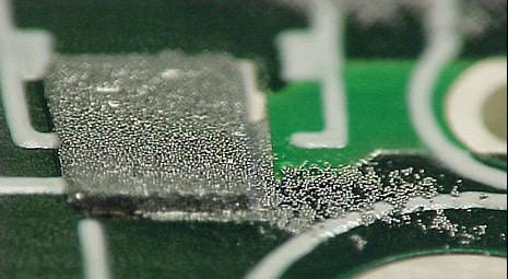
Solder paste bleeding, also known as 'solder-paste-bleed-out', is a defect that can occur during the solder paste printing process. This defect involves the unintentional seepage or spreading of solder paste beyond the intended pad areas on the PCB, often between the stencil and the PCB itself. Solder paste bleeding can result in poor solder joint quality and negatively impact the functionality and reliability of electronic assemblies.
Causes of Solder Paste Bleeding:
Solder paste bleeding can occur due to various factors and process-related issues, including:
- Stencil Aperture Design: The design of the stencil apertures, including their size, shape, and spacing, can significantly influence the likelihood of solder paste bleeding. Inadequate stencil design may not adequately control the flow of solder paste.
- Stencil Thickness: The thickness of the stencil can affect the amount of solder paste applied. If the stencil is too thin or flexible, it may not maintain the correct distance between the stencil and the PCB, allowing solder paste to bleed out.
- PCB Support: If PCB's are not fully supported, excessive solder paste can be deposited onto the PCB's - this will provide high risk of bleed-out, especially with thin PCB's.
- Squeegee Pressure and Speed: The pressure applied by the squeegee during the solder paste printing process, as well as the speed at which it moves, can affect the consistency of solder paste deposition. Excessive pressure or speed may cause solder paste to bleed out.
- Solder Paste Viscosity: The viscosity of the solder paste can influence its flow characteristics during the printing process. Solder paste with low viscosity may be more prone to bleeding.
- Stencil Alignment: Proper alignment and registration of the stencil with the PCB are crucial. Misalignment can lead to solder paste being squeezed out from under the stencil.
Impact of Solder Paste Bleeding:
Solder paste bleeding can have negative consequences on the SMT assembly process and the quality of electronic assemblies:
- Short Circuits: Solder paste bleeding between adjacent pads can result in unintended electrical connections, causing short circuits and malfunctions.
- Stencil Contamination: Excessive solder paste bleed-out can contaminate the stencil and printing equipment, leading to inconsistent solder paste deposition.
Preventing and Addressing Solder Paste Bleeding:
To prevent and address solder paste bleeding issues in SMT assembly, consider the following strategies:
- Stencil Optimization: Ensure that the stencil design, including aperture size, shape, and spacing, is well-optimized for the components being placed on the PCB. Adequate stencil design can minimize the risk of solder paste bleeding.
- Stencil Thickness: Choose an appropriate stencil thickness based on the solder paste type and printing equipment to achieve consistent solder paste deposition.
- PCB Support: If PCB's are large and/or thin, they will need support to enable a good and repeatable solder paste print. This can be a challenge for double sided assemblies.
- Squeegee Control: Control the squeegee pressure and speed to achieve uniform solder paste printing. Proper alignment and calibration of the printing equipment are essential.
- Solder Paste Viscosity: Use solder paste with the appropriate viscosity for your specific application and printing equipment. This can help ensure that the paste remains within the intended pad areas.
- Stencil Alignment: Ensure precise and accurate alignment and registration of the stencil with the PCB to prevent solder paste from bleeding out.
- Stencil Cleaning: Maintain proper stencil cleanliness to prevent residual solder paste from interfering with the printing process.
- Solder Paste Inspection (SPI): Implement solder paste inspection equipment to monitor and detect any defects or irregularities in solder paste deposition immediately after printing. SPI can help identify and address bleeding issues in real time.
- Process Optimization: Continuously monitor and optimize the solder paste printing process to minimize the occurrence of bleeding and other defects.
By implementing these strategies and maintaining strict process controls, manufacturers can significantly reduce the risk of solder paste bleeding and improve the overall quality and reliability of their electronic assemblies.
