|
|
Solder voiding is a common phenomenon within the surface mount process and affects all smt components with some more affected than others. A solder void is defined as a hole or enclosed volume of space within a solder joint that lacks solder material.
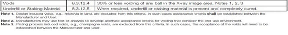
Generally the acceptability for the amount and size of solder voids is simply to be specified by customer/vendor agreement. According to IPC guidelines for a class 2 product, IPC-A-610 defines BGA solder voids to be a defect when the cumulative projected area of all voids in any given solder ball is greater than 30% in an x-ray image.
Generally the acceptability for the amount and size of solder voids is simply to be specified by customer/vendor agreement. According to IPC guidelines for a class 2 product, IPC-A-610 defines BGA solder voids to be a defect when the cumulative projected area of all voids in any given solder ball is greater than 30% in an x-ray image.
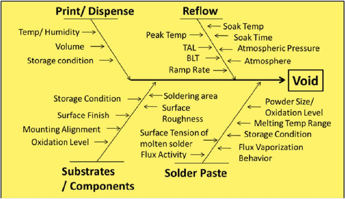
Cause and Effect Diagram for Voids in Solder Joints
|
There are many factors that can influence voiding such as Stencil Design, Reflow Profile, Solder Paste, PCB Design, PCB Surface Finish & Process Environment.
One of the main methods to reduce voiding underneath surface mount components is to increase the number of ‘outgassing’ paths for volatiles to escape. Below are five different stencil aperture designs for a DPAK surface mount component which deposit different volumes of solder paste and which have different 'outgassing' paths:-
One of the main methods to reduce voiding underneath surface mount components is to increase the number of ‘outgassing’ paths for volatiles to escape. Below are five different stencil aperture designs for a DPAK surface mount component which deposit different volumes of solder paste and which have different 'outgassing' paths:-

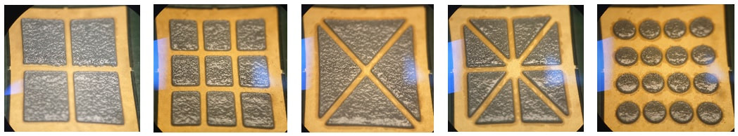
After testing these designs it does show that increasing the 'outgassing' paths does reduce the amount of voiding present and that the design on the right did give the best results - 4 aperture designs gave approx. 40% voiding, 8 & 9 aperture designs gave approx. 30-35% voiding and 15 aperture design gave approx. 25% voiding.
The reflow profile does make a significant difference with a time above liquidus at the upper end of the specification giving the best results - This allows the most time for the volatile materials to escape before the solder joint solidifies.
The solder paste chosen can also make a big difference to the amount of voiding - low temperature lead free solder tends to give very low voiding results as detailed here.
|
Return to home page
|
