|
The choice of stencil thickness for solder paste printing depends on several factors, including the components being assembled, the type of solder paste, the printing equipment, and the desired solder joint quality. Here are some general guidelines to help you determine the appropriate stencil thickness:
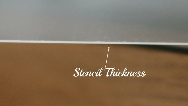
In general, stencil thicknesses for solder paste printing typically range from 0.1 mm (4 mils) to 0.3 mm (12 mils), with variations in between. It's common to start with a stencil thickness that is slightly thinner than the nominal aperture size and adjust as needed through experimentation and testing. Additionally, stencil manufacturers and suppliers may offer guidance and recommendations based on specific solder paste formulations and equipment.
Ultimately, the best stencil thickness for your application should be determined through process optimization, testing, and validation to ensure consistent and high-quality solder paste printing results.
- Component Type and Size: Consider the size and type of components on the PCB. Fine-pitch components with small pads require thinner stencils to ensure accurate solder paste deposition. Larger components with bigger pads may benefit from thicker stencils to ensure adequate solder volume.
- Solder Paste Type: The type of solder paste you are using can influence stencil thickness. Fine-pitch solder pastes with smaller powder sizes may work well with thinner stencils, while coarser solder pastes may require thicker stencils to achieve proper paste release.
- Printed Circuit Board (PCB) Design: The PCB design, including pad sizes, spacing, and component orientation, can impact stencil thickness requirements. Ensure that the stencil thickness matches the PCB layout and pad designs.
- Stencil Aperture Size and Shape: The size and shape of the stencil apertures (or openings) directly affect the solder paste deposition. Thicker stencils may be needed for larger apertures, while thinner stencils are suitable for finer features.
- Solder Paste Printing Equipment: The capabilities of your solder paste printing equipment, such as the type of printer and the alignment accuracy, can influence stencil thickness requirements. Some printers may be better suited for fine-pitch printing with thinner stencils.
- Solder Joint Quality: Consider the desired solder joint quality and reliability for your application. Thicker stencils may provide greater solder volume and improved wetting, while thinner stencils can help prevent excess solder paste deposition.
- Solder Paste Viscosity: The viscosity of the solder paste can impact its flow through the stencil apertures. Thicker stencils may be chosen to accommodate higher-viscosity solder pastes.
- Printing Process Control: Thicker stencils may offer more forgiving printing processes by reducing the risk of bridging between fine-pitch components, while thinner stencils may require more precise setup and control.
In general, stencil thicknesses for solder paste printing typically range from 0.1 mm (4 mils) to 0.3 mm (12 mils), with variations in between. It's common to start with a stencil thickness that is slightly thinner than the nominal aperture size and adjust as needed through experimentation and testing. Additionally, stencil manufacturers and suppliers may offer guidance and recommendations based on specific solder paste formulations and equipment.
Ultimately, the best stencil thickness for your application should be determined through process optimization, testing, and validation to ensure consistent and high-quality solder paste printing results.
|
Return to home page
|
