|
Aspect Ratio vs Area Ratio
Aspect ratio and area ratio are two different parameters used to characterize stencil apertures in electronics assembly, particularly in the context of solder paste printing. They serve different purposes and provide distinct information about the stencil design. Here's an explanation of each:
In summary, while both aspect ratio and area ratio are related to stencil apertures in electronics assembly, they focus on different aspects of the stencil design:
Both parameters are important considerations in stencil design to achieve high-quality and reliable solder paste printing results. Balancing the aspect ratio and area ratio is crucial to ensure that solder paste is deposited accurately and consistently, especially for fine-pitch components and complex PCB layouts.
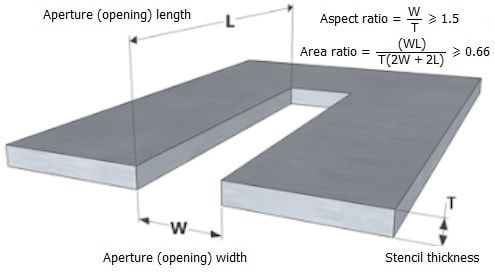
- Aspect Ratio of Stencil Apertures:
- Definition: The aspect ratio of stencil apertures is the ratio of the aperture height (usually the stencil thickness) to the aperture width or diameter. It is expressed as:
Aspect Ratio = Aperture Height (Stencil Thickness) / Aperture Width or Diameter - Purpose: The aspect ratio provides information about the relative size of the stencil apertures in terms of height compared to their width or diameter. It helps assess how challenging it might be to achieve consistent solder paste deposition through the apertures. High aspect ratios (tall and narrow apertures) may pose challenges in paste transfer, especially for fine-pitch components.
- Definition: The aspect ratio of stencil apertures is the ratio of the aperture height (usually the stencil thickness) to the aperture width or diameter. It is expressed as:
- Area Ratio of Stencil Apertures:
- Definition: The area ratio of stencil apertures is the ratio of the area of the aperture opening (width or diameter) to the area of the pad on the printed circuit board (PCB). It is expressed as:
Area Ratio = Aperture Area / Pad Area - Purpose: The area ratio provides information about the relative size of the stencil apertures in terms of their area compared to the pad they are intended to deposit solder paste onto. It helps ensure that the right amount of solder paste is deposited on the PCB pad. The area ratio is critical for achieving proper solder joint volume and avoiding issues like insufficient or excess solder paste.
- Definition: The area ratio of stencil apertures is the ratio of the area of the aperture opening (width or diameter) to the area of the pad on the printed circuit board (PCB). It is expressed as:
In summary, while both aspect ratio and area ratio are related to stencil apertures in electronics assembly, they focus on different aspects of the stencil design:
- Aspect Ratio emphasizes the geometric shape of the aperture, specifically the height relative to the width or diameter. It is concerned with how easily solder paste can flow through the apertures.
- Area Ratio emphasizes the relationship between the aperture size and the size of the PCB pad. It ensures that the correct amount of solder paste is deposited onto the pad for solder joint formation.
Both parameters are important considerations in stencil design to achieve high-quality and reliable solder paste printing results. Balancing the aspect ratio and area ratio is crucial to ensure that solder paste is deposited accurately and consistently, especially for fine-pitch components and complex PCB layouts.
|
Return to home page
|
