What do you think of low temperature lead free solder paste? |
|
The use of low temperature lead free solder paste is becoming more common within the surface mount industry. Certain components cannot handle the peak temperatures necessary for lead-free soldering which typically reaches 240 – 250 °C. These high temperatures can also cause damage to the PCB material such as delamination. Indium and bismuth can be used to lower the melting points of tin-based solders. The melting ranges and peak reflow temperatures of several solder alloys are shown in the table below.
Tin / indium 52% and tin / bismuth 58% are lead free solders that have substantially lower melting points than tin / lead 37% solder. Tin / bismuth and tin / bismuth / silver are the most common choices for low melting lead free solder pastes. The peak reflow temperatures provided by tin / bismuth alloys are low (160 – 170 °C) as compared to tin / lead solders (210 – 220 °C). These low peak temperatures allow for soldering of thermally sensitive assemblies.
Caution must be used when using tin / bismuth alloys. It is dangerous to mix tin / bismuth with lead containing alloys. Tin, bismuth, and lead can form a very low melting combination that melts around 95 °C. This could potentially lead to solder joint failure due to natural heating of the assembly during use.
Tin / bismuth alloys are safe to use in combination with other lead free tin-based alloys. In some cases surface mount assemblies are made with SAC305 on the first side and tin / bismuth on the second side. The low reflow temperature for tin / bismuth minimizes intermetallic growth in the SAC305 solder joints and allows for soldering of thermally sensitive components.
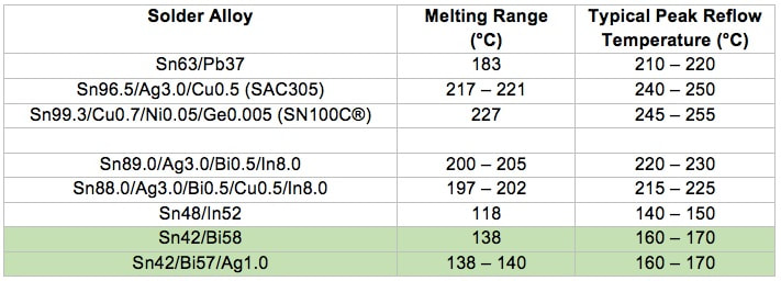
Low Voiding
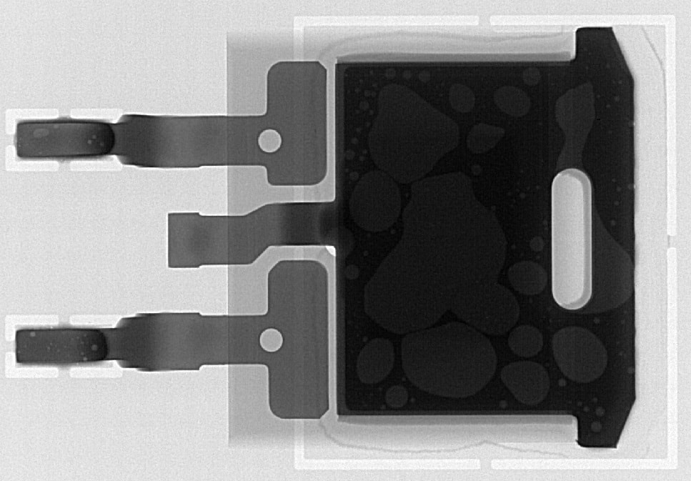
Void formation under components with large soldering planes and low stand-off heights, such as DPAK components, is a well-known phenomenon. These air pockets can reduce mechanical strength as well electrical and thermal conductivity. For Sn(Ag)Cu-based alloys, voiding levels are typically in between 10% and 35% but can be greater than 50%. By using low temperature lead free solder voiding levels can be reduced to less than 10% as can be seen below - click here for more details on voiding.
High level Voiding
|
Low level Voiding
|
|
Return to Home Page
|
