CAD EXTRACTION FROM PCB DESIGN SOFTWARE |
|
ORCAD
Data Extraction up to Version 1.5
To convert a printed circuit board, the database must be extracted as an ASCII file.
To extract an ASCII file from OrCAD Layout for Windows:
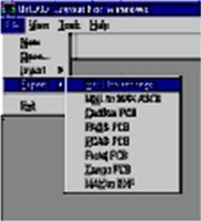
Go into File Menu | Export. Highlight the file format which is to be exported from the list. The OrCAD Layout for Windows format is MAX and to be exported into Test Expert the user should choose MAX Interchange.
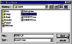
In the editor MAX Board input, highlight the
name of the .max file to be imported.
In the example BUDDY_F1.max
Click on Open.
name of the .max file to be imported.
In the example BUDDY_F1.max
Click on Open.
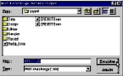
The transition to the MAX Interchange
Notation Output Editor is automatic.
The name of the highlighted file is in the file
name edit box and by default it is given the suffix
.min. Click Save.
Notation Output Editor is automatic.
The name of the highlighted file is in the file
name edit box and by default it is given the suffix
.min. Click Save.
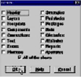
In the Options Editor, check the box "All of the above" to process everything in the file.
Click the OK button.
Click the OK button.
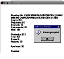
When the processing is completed the MIN Back
Annotation Editor displays data relevant to the PCB
such as:
Original file name and location.
Destination name and location.
Number of layers, padstacks, nets, etc.
If any errors occurred.
Click OK to return to the OrCAD Layout for Windows
screen.
Annotation Editor displays data relevant to the PCB
such as:
Original file name and location.
Destination name and location.
Number of layers, padstacks, nets, etc.
If any errors occurred.
Click OK to return to the OrCAD Layout for Windows
screen.
An Orcad MIN file looks something like this :
(MIN
(Version 5004)
(MajorRev 7)(MinorRev 0)
(L 28)(V 16)
(Begin
(Header
(Grid 500)
(MIN
(Version 5004)
(MajorRev 7)(MinorRev 0)
(L 28)(V 16)
(Begin
(Header
(Grid 500)
ORCAD Version 16 onwards
These versions of Orcad share a common Graphical User Interface with Cadence Allegro and require the use of specific scripts to output specific data requirements.
See the requirements for Cadence Allegro.
These versions of Orcad share a common Graphical User Interface with Cadence Allegro and require the use of specific scripts to output specific data requirements.
See the requirements for Cadence Allegro.
CADENCE ALLEGRO
Data Extraction
There are 2 possibilities for extracting data from Cadence Allegro (and also latest version of Cadence ORCAD), both of which require the CAD engineer to run a special script ON the CAD system - it is NOT possible to do this after data has been extracted as all Cadence data is extracted using customised script programs.
i) ODB++
Cadence have brought Orcad into line with Allegro such that they are using a common GUI for Layout/PCB design and that their "favourite" export of data is the "Allegro way" which is to use script programs for specific formats and that they have a "valued tie-in" with Valor for ODB++ which means that you have to download a utility script from Valor.
On the CADS system GUI there Is a special link ‘Export -ODB inside’.
If not present already this prompts the user to download the Valor ODB script writer which then prompt the user to open the job file and produce the ODB output. The CAD user must take care to select ALL layer options, FULL file otherwise it will produce a ‘cut-down’ file for Assembly usage only and not including items like the netlist and net connections.
ii) Using the TestExpert CDC2FAB provided script program.
To convert a printed circuit board from an ALLEGRO CAD system, the database must first be extracted as an ASCII file using the CADENCE ALLEGRO Data Extract utility which is controlled by the Test Expert script file.
The Test Expert script file describes the data to be extracted from the database.. Please see the documentation for the Windows extraction program (CDS2FAB) if you have a Windows-based version of CADENCE.
This script formats the data in a VERY specific way, which means that the file extracted using one Company's script will NOT work with another Company's software because although they may look 'similar' they are not is the expected format or column order.
Also you cannot simply re-order the columns because we require a number of sections with different information (Part, Net, Package etc etc).
So, in order for Fabmaster/TestExpert to work with Cadence files, we need a single ascii file extracted from Cadence that contains the pcb information.
In order to do this, the customer needs the Fabmaster "extraction script" and instructions. This script must be run on the computer that has Cadence loaded on it.
Windows:
They need to extract this zip folder and it will produce a folder called Fabmaster'. All they need to do is to run the executable CDC2FAB in this file structure. This starts the installation process. It is best to accept the defaults but to check the configuration file paths to the Cadence system libraries etc
Then ask to view the readme file. It's best to print it out. It then tells you how to run the program.
The important thing is to make sure that the final file looks like the sample file attached. A Cadence for Unix file header should look something like this:
A Cadence for Windows file should look something like this:
If the extracted files don't look basically like this, they are not right and it will not import into Fabmaster or TestExpert
Once the file has been produced it is transferred to the Test Expert system and run using the CADENCE input processor.
Once the file has been produced it is transferred to the Test Expert system and run using the CADENCE input processor.
CADSTAR
Data Extraction
Before running the input processor, the CADIF database must be extracted from the CAD system in order to convert a printed circuit board from the CADSTAR for Windows system to Test Expert.
The CADSTAR for Windows system generates an output file in CADIF version 4.0 format with the extension .PAF. To generate the file in CADIF format on the CAD system:
Load the printed circuit board layout (OPEN FILE).
Click the option EXPORT.
When prompted for the format, type CADIF and confirm.
The CADIF format file is then generated using the printed circuit board name with the extension .PAF, for example: cads01.paf.
A Cadstar CADIF/PAF file looks something like this :
EAGLE
This is a very easy extraction to produce Fabmaster FATF or Gencad providing the user has at least Eagle version 4.11.
Use the menu item ‘File - run’ which will open up the User Language Program folder and browse for the ‘fabmaster.ulp’ file.
Select open :
This is a very easy extraction to produce Fabmaster FATF or Gencad providing the user has at least Eagle version 4.11.
Use the menu item ‘File - run’ which will open up the User Language Program folder and browse for the ‘fabmaster.ulp’ file.
Select open :
and you should then see the message ‘Run: fabmaster.ulp : finished’ on the bottom of the Eagle window :
It will have created a file with a ‘fab’ extension in the project folder where the board data is stored. This can be transferred to Test Expert and imported using the FATF input processor.
If you prefer as an alternative there is a GENCAD-2 ULP available, but this is not installed by default so you will have to get this from the Download section of the CADSOFT website.
If you prefer as an alternative there is a GENCAD-2 ULP available, but this is not installed by default so you will have to get this from the Download section of the CADSOFT website.
PULSONIX
i) Pulsonix ODB++ export
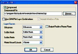
To export ODB++, data got to the menu Output - ODB++ in the window that opens, check the ‘Compressed’ box to generate the files into a compressed ‘tgz’ structure.
Do not check the ‘Use CAM/Plot Layer Combinations as this will not generate ALL the layers but will only output a sub-set as defined in the options settings :
ii) Pulsonix Gencad export
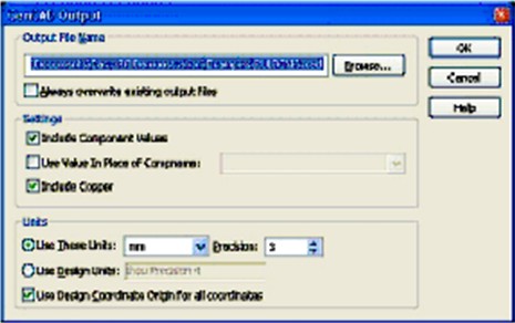
From the Output menu, select the GenCAD option (this is a purchasable add-on option for this system), the dialog below is similar to that displayed below:
From the Output menu, select the GenCAD option (this is a purchasable add-on option for this system), the dialog below is similar to that displayed below:
From this dialog, you can choose the name of the output file to be generated. The default for this name is the same as the name of your PCB design, with the file extension for GenCAD files as defined in the Options dialog.
EASYPC
i) EasyPC ODB++ export
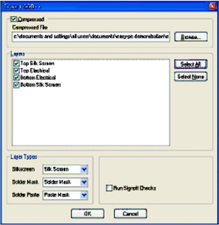
To export ODB++, data got to the menu Output - ODB++ in the window that opens, check the ‘Compressed’ box and ‘Select All’ layers :
i) EasyPC ODB++ export
To export ODB++, data got to the menu Output - ODB++ in the window that opens, check the ‘Compressed’ box and ‘Select All’ layers :
Choose where you want to save the file using the browse entry box and this will create a compressed ‘tgz’ file which can be processed using the Test Expert ODB++ input processor.
ii) EasyPC Gencad export
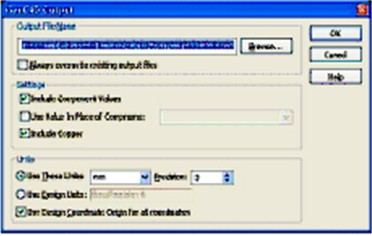
To produce GENCAD from the menu Output - Export Gencad, select ‘Include Component values’ and ‘Include Copper’.
It will default to using units ‘mm’ and ‘Use Design Coordinate Origin for all coordinates’, which are okay for Test Expert.
Use the browse entry box to name the file and choose the folder location where you wish to save to. This will produce a Gencad file with a file extension of ‘cad’ which can be processed using the Test Expert Gencad input processor.
PADS
Data Extraction
Before running the input processor, the database must be extracted from the PADS PCB CAD system as an ASCII file and transferred to the system where Test Expert is installed.
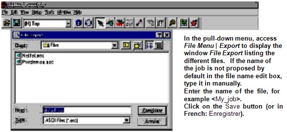
To output an ASCII database from a PADS PCB CAD system: Select the menu: IN/OUT.
Select ASCII OUT.
Select the option: ALL.
Select GO.
These instructions will generate an ASCII output file with the extension .ASC.
This file should be renamed .PAD before it is transferred to prevent confusion with other file names used by Test Expert.
A sample listing of the contents of this file is supplied at the end of the datasheet.
Note re PADS POWER SUITE
If using the PADS POWER Suite release, do NOT output the file in BASIC. Instead, use Mils.
A sample of the header file follows.
Example: Generating an ASCII File Using PADS PowerPCB V.1.5
Install the software PADS PowerPCB on the system where Test Expert has been set up.
Install the software PADS PowerPCB on the system where Test Expert has been set up.
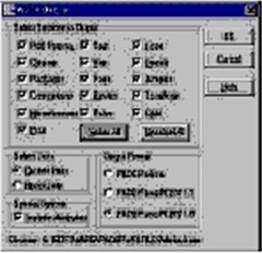
To output an ASCII file containing the necessary
data:
Select Sections to Output
Click the button Select All to check all the sections. Select Units
Select Current Units.
Special Options
Select Include Attributes.
Output Format
Select PADS PowerPCB v1.5
All ‘flavours’ of PADS file format look something like this :
And are all processed using the Test Expert PADS input processor.
NOTE : Use of Solder Mask data with PADS CAD system
Typically without manual intervention to the “Standard” pad or Test points solder resist, the solder relief aperture is generated from the copper pad size, plus an under/oversize pad value that is held within the Gerber output. This is defined as a standard default on the CAD system but may typically be say 3 thou, so a 20 thou pad will have a 23 thou solder relief aperture, but this could vary for different PADS users and for use with different PCB manufacturers. Importantly the data held here is not used until the Gerber files are generated.
Test Expert inputs the PADS ASCII Data and reads the Solder Mask from Layers 21 and 28. In terms of the PADS system, these layers are reserved only for “special” solder resist definitions, which are exceptions to the standard default. An example of this could be on non-plated holes where it is bad practise to have solder resist coating getting into the holes, so the CAD Engineer might manually make the solder resist 5 thou larger than the hole and then this data will be added to Layer 21 and/or Layer 28 in the PADS job.
This means that for Test Expert to make use of the Solder Mask data from PADS, it is recommended that ANY locations that are to be selected for Test Access would need to be treated in the CAD system as an exception to the standard default and would therefore be applied to the 'special' layers 21 and/or 28.
The customer CAD Engineer may have valid reasons not to make these manual changes to the global defaults apart from having to create the exception for every relevant shape, which means additional work. They may use the under/oversize pad feature for different technologies of PCB’s and different manufacturers - A high end PCB (tight pitch components) may have a very small oversize, but on a low end board (large pitch components), they may expand the aperture to allow for less accurate solder mask registration, and the use of cheaper manufacturing methods.
But if these Manual exceptions are not made in the CAD system and then the Test Expert user makes use of the Test Expert Nails Rule for checking potential Nail location to the Solder Mask clearance, allocating Nails/Probing will not be possible at some points on the pcb.
ZUKEN
Before running the input processor, the required data must be extracted from the ZUKEN5 CAD system.
Zuken's CDB software uses binary databases.The two files required for Test Expert are ASCII representations of the database:
.pcf file: ASCII board layout file (placement and layer symbol file, layer count, units, etc.).
.ftf file: the ASCII representation of the footprints used in the design (package description file).
Steps to Extract the Data
Test Expert requires two ASCII files: <basename>.ftf and <jobname>.pcf. To convert a printed circuit board from a ZUKEN CR-5000 system, the user must first extract the database as two ASCII files.
To extract the database as ASCII files this, follow the procedure below:
Convert the binary file <basename>.ftp into an ASCII file. Inside the cdb directory, extract <basename>.ftf using the DOS (or command script) command ftout.exe <basename> (this calls up, for example, C:\cr5000\bin\ftout.exe).
Convert the binary file <jobname>.pcb into an ASCII file. Inside the pcb directory, extract <jobname>.pcf using the DOS (or command script) command pcout.exe <jobname> (this calls up, for example, C:\cr5000\bin\pcout.exe).
The file name (the prefix) must be the same for both files which means the user must rename the <basename>.ftf file using the same name as the <jobname>.ftf file.
Store both (converted) files in a directory named, for example, <jobname> and then zip the CAD files up (<jobname>.zip).
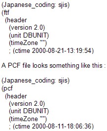
An FTF file looks something like this :
VUTRAX
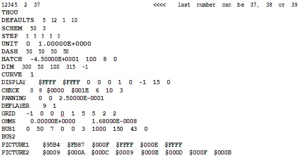
The VUTRAX input processor has currently been tested for use with VUTRAX software release 11 and 12. It is important to note that it only supports files beginning with the header line:
12345 2 37 (this is Version 11)
or
12345 2 38 (this is Version 12)
See the sample file.
If the File begins 12345 2 39 this is Version 13 , in this case the file will need to be converted using free-issue files from Vutrax to downversion to version 12 or version 11. One of the main features supported in version13 is track ‘arcs’ which will be converted to straight lines - this does not affect the integrity of the information for assembly or test purposed.
Data Extraction
Vutrax users can save the CAD job file as a “Draft” output.
By default, the input processor recognises and processes files with the suffix .art.
This file with the suffix .art is extracted from the VUTRAX Graphics PCB design tools.
The file *.art MUST be the pure ASCII version.
The option exists in the Vutrax system where the “Draft” .art file begins in ASCII format and becomes binary format at the end of the file following the line "ENDATTRIB" this is not acceptable
|
Return to home page
|
