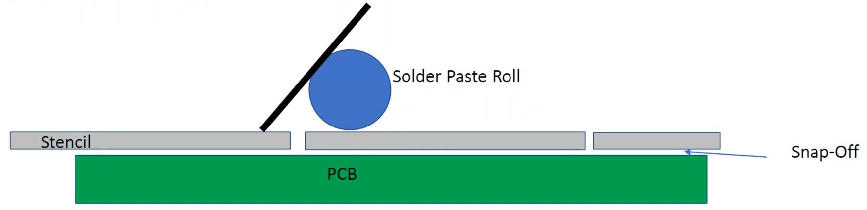
What the differences between 'on-contact' printing and 'gap' printing?
"On-contact printing" and "gap printing" are two different approaches to solder paste printing in the electronics manufacturing process, particularly in surface mount technology (SMT) assembly. Each approach has its own advantages and considerations:
On-Contact Printing:
On-contact printing, as the name suggests, involves making physical contact between the stencil and the PCB. The stencil is pressed directly onto the PCB surface during the printing process.
- Advantages:
- Improved transfer efficiency: Because there is direct contact between the stencil and the PCB, it can result in better transfer of solder paste, leading to more consistent and precise deposits.
- Reduced solder paste smearing: Since there is minimal gap between the stencil and the PCB, there is less chance of solder paste smearing or misalignment during the separation step.
- Better support for fine-pitch components: On-contact printing is often preferred for fine-pitch and ultra-fine-pitch applications due to its precision.
- Considerations:
- Risk of stencil wear: Frequent stencil contact can lead to wear and may require more frequent stencil replacement.
- Limited compatibility with warped PCBs: On-contact printing may not be suitable for PCBs with warping or uneven surfaces.
- Risk of stencil wear: Frequent stencil contact can lead to wear and may require more frequent stencil replacement.
Gap Printing:
Gap printing involves maintaining a controlled gap or distance between the stencil and the PCB during the printing process. The solder paste is dispensed through the gap and onto the PCB.
- Advantages:
- Reduced stencil wear: Gap printing typically results in less wear on the stencil because it avoids the constant contact seen in on-contact printing.
- Suitable for warped PCBs: Gap printing can better accommodate PCBs with uneven or warped surfaces because the stencil does not make direct contact with the PCB.
- Considerations:
- Potential for reduced transfer efficiency: Maintaining a gap introduces the possibility of reduced transfer efficiency, as there may be more inconsistencies in solder paste deposition compared to on-contact printing.
- Higher risk of solder paste smearing: A larger gap can result in more potential for solder paste smearing or misalignment during separation.
- Limited suitability for fine-pitch components: Gap printing may be less precise and, therefore, less suitable for very fine-pitch components or applications.
The choice between on-contact and gap printing depends on the specific requirements of the PCB assembly, the characteristics of the solder paste, the design of the stencil, and the equipment used. Many manufacturers employ a combination of these approaches or may switch between them based on the specific demands of the PCB being assembled. The goal is to achieve the best solder paste deposition for high-quality and reliable solder joints.
