SURFACE MOUNT PROCESS
  • Home
  • Articles
    • A GUIDE TO EFFECTIVE STENCIL DESIGN
    • SOLDER PASTE PRINTING PROCESS
    • SOLDER PASTE INSPECTION PROCESS
    • COMPONENT PLACEMENT PROCESS
    • REFLOW SOLDERING PROCESS
    • POST-REFLOW AOI PROCESS
    • THROUGH-HOLE ASSEMBLY - SELECTIVE SOLDERING
    • Cleaning 'No-Clean' flux residues and other contaminants
    • Environmental Protection - Conformal Coating
    • Hand soldering and rework of surface mount components to IPC class 3
  • FAQ
    • Solder paste handling
    • Type 3 or Type 4 Solder Paste
    • Cleaning a misprinted PCB
    • Solder Paste Quality Control
    • What factors affect solder paste transfer efficiency
    • What stencil thickness should be used?
    • What is the difference between aspect ratio and area ratio of stencil apertures?
    • What squeegee speed should be used?
    • What squeegee pressure should be used?
    • What the differences between 'on-contact' printing and 'gap' printing?
    • What separation speed to use in solder paste printing?
    • What are the benefits / challenges of using halogen-free solder paste?
    • What is the best stencil aperture shape for solder paste transfer efficiency?
    • PCB delamination during reflow
    • What are the different types of reflow profile?
    • ROSE (Resistivity of Solvent Extract) testing
    • How do you validate a PCBA cleaning process?
    • Why clean a pcba that has been soldered using no-clean flux
    • How do engineered cleaning fluids such as Zestron and Kyzen work
    • How do engineered cleaning fluids affect surface tension and wetting angle?
    • How does the pH level affect engineered cleaning fluids?
    • How do mixed-bed and carbon filters work in PCB cleaning systems?
    • What are the risks of using ultrasonics to clean PCBA's?
    • What are the differences between 'Water-soluble' and 'No-clean' flux?
    • What is the difference between ionic and non-ionic contamination?
    • What causes electrochemical migration (ECM)?
    • What are methods of masking before conformal coating?
    • How to apply conformal coating by brushing?
    • How to apply conformal coating using dipping?
    • How to apply conformal coating using spray/aerosol?
    • How do selective robots apply conformal coating?
    • What is the best method to dry/cure conformal coating?
    • What concerns are there when demasking?
    • What should be checked when inspecting after conformal coating?
    • How to check the adhesion of conformal coating?
    • Tape and Reel Packaging Standards
    • What is 'Package on Package' (POP)?
    • Stock control and component attrition
    • BOM Comparison Software
    • Comparison of SAC305 and SAC387 Lead-Free Solder Alloys
    • What is a 'Eutectic' solder alloy?
    • What does 'SMT' stand for?
    • What does the term voiding mean?
    • How is void percentage calculated?
    • How to reduce voids in QFN device ground connection?
    • Low temperature lead free solder paste
    • CAD EXTRACTION
    • How are PCB's manufactured?
    • What are the IPC standards that govern electronics manufacturing processes?
    • What are the differences between SMEMA and HERMES?
  • Contact
  • Store

What should be checked when inspecting after conformal coating?

Picture
Conformal coating is a protective layer applied to electronic components and printed circuit boards (PCBs) to protect them from environmental factors such as moisture, dust, chemicals, and temperature extremes. After the conformal coating process, it is crucial to perform a thorough inspection to ensure the coating has been applied correctly and that there are no defects that could compromise the integrity of the electronic assembly. Here are some steps typically involved in the inspection after conformal coating:
  1. Visual Inspection:
    • Examine the coated surface for uniform coverage. Ensure there are no areas with insufficient coating or excessive buildup.
    • Check for any bubbles, pinholes, or voids in the coating. These can potentially allow contaminants to penetrate the coating.
  2. Thickness Measurement:
    • Measure the coating thickness at various locations using a coating thickness gauge. Ensure that the thickness meets the specified requirements.
  3. Cure Check:
    • Verify that the conformal coating has cured properly. Inadequate curing can lead to issues such as poor adhesion and chemical resistance.
  4. Edge Coverage:
    • Inspect the edges of components and PCBs to ensure that the conformal coating adequately covers and protects these areas.
  5. Masking Removal Check:
    • If masking was used during the coating process to protect certain areas, ensure that the masking has been removed completely and that there is no residue left behind.
  6. Dielectric Strength Test:
    • Conduct dielectric strength tests to ensure that the conformal coating provides the necessary insulation properties.
  7. Adhesion Test:
    • Perform adhesion tests to evaluate the bonding strength between the conformal coating and the substrate. This ensures that the coating will not delaminate over time.
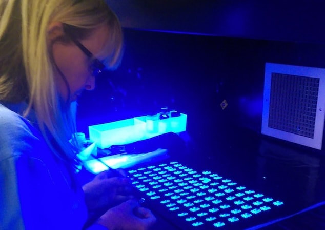
  8. UV Inspection (for UV-cured coatings):
    • If the conformal coating is UV-cured, use UV light to inspect for any inconsistencies or defects that may not be visible under normal lighting conditions.
  9. Functional Testing:
    • Depending on the application, perform functional testing of the electronic components to ensure that the conformal coating does not negatively impact the performance.
  10. Documentation:
    • Maintain detailed records of the inspection process, including measurements, test results, and any corrective actions taken.
By performing a comprehensive inspection after conformal coating, you can help ensure the reliability and longevity of the electronic assemblies in various environments. If any issues are identified during the inspection, appropriate corrective actions should be taken to address them.
© COPYRIGHT 2015. ALL RIGHTS RESERVED.