
THROUGH HOLE TROUBLSHOOTING GUIDE
|
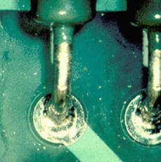
Insufficient Hole Fill
Possible Causes: Inadequate flux, topside PCB temperature too low, wave height to low, lead-to-hole ratio too small, PCB contains solder joints connected to internal ground planes.
Preventive Actions: Verify flux deposition, verify preheat temperature, check wave height, check lead-to-hole aspect ratio, verify internal ground planes |
|
Insufficient Wetting
Possible Causes: Inadequate flux, dwell time too short, topside PCB temperature too low, poor solderability, contamination
Preventive Actions: Verify flux deposition, reduce drag speed/Increase solder time, verify preheat temperature, check component for contamination, check board contamination |
|
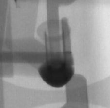
Blow Holes and Voids
Possible Causes: Topside PCB temperature too low, flux carrier outgassing, moisture in PCB, poor through-hole plating
Preventive Actions: Verify topside PCB temperature, verify flux deposition and required preheat temperature, check for moisture in laminate - prebake if necessary, check though-hole plating |
|
Solder Bridging
Possible Causes: Protruding lead length too long, inadequate flux, solder drag speed too fast, nozzle peel-off movement
Preventive Actions: Reduce lead protrusion length, verify flux deposition, decrease drag speed, re-program peel-off movement |

|
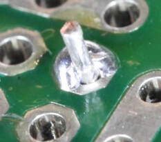
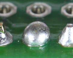
Solder Balls (Attached firmly to solder mask)
Possible Causes: Excessive flux, topside PCB temperature too
low, solder temperature too high, solder mask porosity Preventive Actions: Reduce amount of flux, verify topside PCB temperature, consider using lower temperature lead-free alloy, consider alternative solder mask material |
|
Sunken Solder Joints
Possible Causes: Lead-to-hole ratio too large, moisture in PCB, flux carrier outgassing, topside PCB temperature too low, poor through-hole plating, poor solderability
Preventive Actions: Reduce lead-to-hole ratio, check for moisture in laminate - prebake if necessary, verify topside PCB temperature, check though-hole plating, check component for contamination |
|
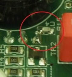
Adjacent Component Solder Short
Possible Causes: Inadequate TH to SMT clearance, lead length too long, solder nozzle movement, solder nozzle peel-off movement
Preventive Actions: Implement keep-out DFMA guidelines, reduce lead protrusion length, re-program nozzle movement, re-program peel-off movement |
|
Excessive Solder
Possible Causes: Protruding lead length too long, inadequate flux, solder drag speed too fast, nozzle peel-off movement
Preventive Actions: Reduce lead protrusion length, verify flux deposition, decrease drag speed, re-program peel-off movement |
|
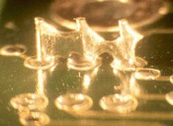
Solder Flags
Possible Causes: Protruding lead length too long, inadequate flux, solder drag speed too fast, nozzle peel-off movement
Preventive Actions: Reduce lead protrusion length, verify flux deposition, decrease drag speed, re-program peel-off movement |
