SURFACE MOUNT PROCESS
  • Home
  • Articles
    • A GUIDE TO EFFECTIVE STENCIL DESIGN
    • SOLDER PASTE PRINTING PROCESS
    • SOLDER PASTE INSPECTION PROCESS
    • COMPONENT PLACEMENT PROCESS
    • REFLOW SOLDERING PROCESS
    • POST-REFLOW AOI PROCESS
    • THROUGH-HOLE ASSEMBLY - SELECTIVE SOLDERING
    • Cleaning 'No-Clean' flux residues and other contaminants
    • Environmental Protection - Conformal Coating
    • Hand soldering and rework of surface mount components to IPC class 3
  • FAQ
    • Solder paste handling
    • Type 3 or Type 4 Solder Paste
    • Cleaning a misprinted PCB
    • Solder Paste Quality Control
    • What factors affect solder paste transfer efficiency
    • What stencil thickness should be used?
    • What is the difference between aspect ratio and area ratio of stencil apertures?
    • What squeegee speed should be used?
    • What squeegee pressure should be used?
    • What the differences between 'on-contact' printing and 'gap' printing?
    • What separation speed to use in solder paste printing?
    • What are the benefits / challenges of using halogen-free solder paste?
    • What is the best stencil aperture shape for solder paste transfer efficiency?
    • PCB delamination during reflow
    • What are the different types of reflow profile?
    • ROSE (Resistivity of Solvent Extract) testing
    • How do you validate a PCBA cleaning process?
    • Why clean a pcba that has been soldered using no-clean flux
    • How do engineered cleaning fluids such as Zestron and Kyzen work
    • How do engineered cleaning fluids affect surface tension and wetting angle?
    • How does the pH level affect engineered cleaning fluids?
    • How do mixed-bed and carbon filters work in PCB cleaning systems?
    • What are the risks of using ultrasonics to clean PCBA's?
    • What are the differences between 'Water-soluble' and 'No-clean' flux?
    • What is the difference between ionic and non-ionic contamination?
    • What causes electrochemical migration (ECM)?
    • What are methods of masking before conformal coating?
    • How to apply conformal coating by brushing?
    • How to apply conformal coating using dipping?
    • How to apply conformal coating using spray/aerosol?
    • How do selective robots apply conformal coating?
    • What is the best method to dry/cure conformal coating?
    • What concerns are there when demasking?
    • What should be checked when inspecting after conformal coating?
    • How to check the adhesion of conformal coating?
    • Tape and Reel Packaging Standards
    • What is 'Package on Package' (POP)?
    • Stock control and component attrition
    • BOM Comparison Software
    • Comparison of SAC305 and SAC387 Lead-Free Solder Alloys
    • What is a 'Eutectic' solder alloy?
    • What does 'SMT' stand for?
    • What does the term voiding mean?
    • How is void percentage calculated?
    • How to reduce voids in QFN device ground connection?
    • Low temperature lead free solder paste
    • CAD EXTRACTION
    • How are PCB's manufactured?
    • What are the IPC standards that govern electronics manufacturing processes?
    • What are the differences between SMEMA and HERMES?
  • Contact
  • Store

How to apply conformal coating using spray/aerosol?

Picture
Conformal coating is a protective material applied to electronic circuitry to protect it from environmental factors such as moisture, dust, chemicals, and temperature extremes. Applying conformal coating by spray and aerosol methods is a common practice in the electronics industry. Here's an overview of the process for both methods:
1. Surface Preparation:
  • Before applying conformal coating, it's crucial to ensure that the surfaces to be coated are clean and free from contaminants such as dust, oils, and residues.
  • Cleaning methods may include using solvents, brushes, or specialized cleaning equipment.
2. Masking:
  • Components that should not be coated, such as connectors, switches, and certain areas of the board, are often masked using tapes or liquid masking materials.
3. Selection of Conformal Coating:
  • Choose the appropriate conformal coating material based on the specific requirements of the application and the environmental conditions the electronics will be exposed to.
  • Common types include acrylics, urethanes, silicones, and epoxies.
4. Mixing (if required):
  • Some conformal coatings come as a two-part system that needs to be mixed before application. Follow the manufacturer's instructions for proper mixing ratios and procedures.
5. Application by Spray:
  • Using a spray gun or automated spray system, the conformal coating is evenly applied to the surface of the PCB (Printed Circuit Board).
  • The spray gun should be held at an optimal distance and moved at a consistent speed to ensure uniform coverage.
6. Application by Aerosol:
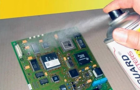
  • Conformal coating in aerosol form is available in cans with a nozzle for direct application.
  • Ensure the aerosol is shaken well before use to mix the coating material properly.
7. Curing:
  • Allow the conformal coating to cure or dry based on the manufacturer's recommendations. This may involve air drying, heat curing, or UV curing depending on the type of coating used.
8. Inspection:
  • After the conformal coating has cured, inspect the coated surface for uniformity, coverage, and the absence of defects.
  • Special attention should be given to areas near masked components to ensure there are no coating bridges or voids.
9. Testing:
  • Perform electrical testing to ensure that the conformal coating has not adversely affected the functionality of the electronic components.
10. De-masking (if applied):
  • Remove any masking materials that were applied before coating.
11. Final Inspection:
  • Conduct a final inspection to ensure that the conformal coating meets the desired standards and provides the necessary protection.

As this is a semi-skilled process, training is vital for a consistent process.  Following proper procedures and guidelines from the conformal coating material manufacturer is essential to achieve optimal results and ensure the reliability of the coated electronic assemblies.
© COPYRIGHT 2015. ALL RIGHTS RESERVED.