SURFACE MOUNT PROCESS
  • Home
  • Articles
    • A GUIDE TO EFFECTIVE STENCIL DESIGN
    • SOLDER PASTE PRINTING PROCESS
    • SOLDER PASTE INSPECTION PROCESS
    • COMPONENT PLACEMENT PROCESS
    • REFLOW SOLDERING PROCESS
    • POST-REFLOW AOI PROCESS
    • THROUGH-HOLE ASSEMBLY - SELECTIVE SOLDERING
    • Cleaning 'No-Clean' flux residues and other contaminants
    • Environmental Protection - Conformal Coating
    • Hand soldering and rework of surface mount components to IPC class 3
  • FAQ
    • Solder paste handling
    • Type 3 or Type 4 Solder Paste
    • Cleaning a misprinted PCB
    • Solder Paste Quality Control
    • What factors affect solder paste transfer efficiency
    • What stencil thickness should be used?
    • What is the difference between aspect ratio and area ratio of stencil apertures?
    • What squeegee speed should be used?
    • What squeegee pressure should be used?
    • What the differences between 'on-contact' printing and 'gap' printing?
    • What separation speed to use in solder paste printing?
    • What are the benefits / challenges of using halogen-free solder paste?
    • What is the best stencil aperture shape for solder paste transfer efficiency?
    • PCB delamination during reflow
    • What are the different types of reflow profile?
    • ROSE (Resistivity of Solvent Extract) testing
    • How do you validate a PCBA cleaning process?
    • Why clean a pcba that has been soldered using no-clean flux
    • How do engineered cleaning fluids such as Zestron and Kyzen work
    • How do engineered cleaning fluids affect surface tension and wetting angle?
    • How does the pH level affect engineered cleaning fluids?
    • How do mixed-bed and carbon filters work in PCB cleaning systems?
    • What are the risks of using ultrasonics to clean PCBA's?
    • What are the differences between 'Water-soluble' and 'No-clean' flux?
    • What is the difference between ionic and non-ionic contamination?
    • What causes electrochemical migration (ECM)?
    • What are methods of masking before conformal coating?
    • How to apply conformal coating by brushing?
    • How to apply conformal coating using dipping?
    • How to apply conformal coating using spray/aerosol?
    • How do selective robots apply conformal coating?
    • What is the best method to dry/cure conformal coating?
    • What concerns are there when demasking?
    • What should be checked when inspecting after conformal coating?
    • How to check the adhesion of conformal coating?
    • Tape and Reel Packaging Standards
    • What is 'Package on Package' (POP)?
    • Stock control and component attrition
    • BOM Comparison Software
    • Comparison of SAC305 and SAC387 Lead-Free Solder Alloys
    • What is a 'Eutectic' solder alloy?
    • What does 'SMT' stand for?
    • What does the term voiding mean?
    • How is void percentage calculated?
    • How to reduce voids in QFN device ground connection?
    • Low temperature lead free solder paste
    • CAD EXTRACTION
    • How are PCB's manufactured?
    • What are the IPC standards that govern electronics manufacturing processes?
    • What are the differences between SMEMA and HERMES?
  • Contact
  • Store

How to apply conformal coating using dipping?

Picture
Applying conformal coating by dipping is a common method used to protect electronic components from environmental factors such as moisture, chemicals, dust, and other contaminants. The process involves immersing the electronic assembly into a liquid conformal coating material and then allowing it to drain and cure. Here's a step-by-step explanation of the dipping process:
  1. Cleaning the PCB (Printed Circuit Board):
    • Before dipping, it is crucial to ensure that the PCB is thoroughly cleaned to remove any residues, flux, or contaminants that might interfere with the adhesion of the conformal coating.
  2. Masking:
    • Components that should not be coated, such as connectors, switches, and certain sensitive devices, are usually masked off using masking tapes or other protective materials.
  3. Selection of Conformal Coating Material:
    • Choose the appropriate conformal coating material based on the specific requirements of the application. Common types include acrylics, urethanes, silicones, and epoxy-based coatings.
  4. Viscosity Check:
    • Ensure that the viscosity of the conformal coating material is suitable for the dipping process. Viscosity affects the coating thickness and can be adjusted by thinning the material if necessary.
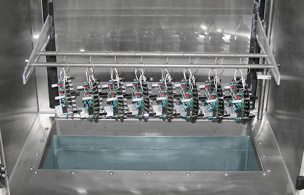
  5. Dipping Process:
    • The PCB is immersed into the liquid conformal coating material. The immersion can be done manually or with the help of automated equipment designed for this purpose.
  6. Draining:
    • After immersion, the PCB is lifted out of the coating material, allowing excess coating to drain off. The draining process helps control the coating thickness and prevents the formation of drips or uneven coatings.
  7. Curing:
    • The coated PCB is then allowed to cure. The curing time and conditions depend on the type of conformal coating material being used. Common curing methods include air drying, thermal curing, or exposure to ultraviolet (UV) light.
  8. Inspection:
    • Once cured, the coated PCB undergoes inspection to ensure uniform coverage, absence of defects, and compliance with the specified coating thickness. Various inspection techniques, including visual inspection and testing for electrical functionality, may be employed.
  9. Removal of Masking:
    • If masking was applied, it is carefully removed to expose the protected areas.
  10. Final Inspection and Testing:
    • A final inspection is performed to confirm that the conformal coating process meets the required standards. Electrical testing may also be conducted to ensure that the coated components function as intended.

It's important to follow the manufacturer's guidelines for the specific conformal coating material being used and to consider the environmental and electrical requirements of the electronic assembly.
© COPYRIGHT 2015. ALL RIGHTS RESERVED.