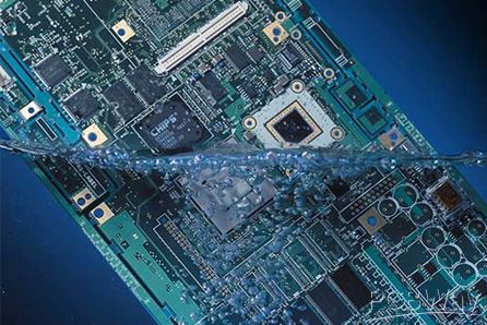
Cleaning PCBA (Printed Circuit Board Assemblies) that have been soldered using no-clean flux is a decision that depends on specific factors and application requirements. While no-clean fluxes are formulated to leave behind residues that are non-corrosive and non-conductive, there are situations where cleaning may still be necessary or beneficial:
Reliability and Longevity: Even though no-clean flux residues are generally designed to be stable and reliable, some applications, especially those with stringent reliability requirements (e.g., aerospace, medical devices, automotive), may demand the utmost cleanliness to ensure long-term performance and avoid potential issues related to corrosion or electrical leakage.
Surface Quality: In some cases, the visual appearance of a PCB is critical, and the presence of flux residues can affect the board's aesthetics. For consumer electronics or products with transparent or exposed PCBs, cleanliness is a concern.
Compatibility: When conformal coatings, potting compounds, or other post-assembly treatments are applied to the PCB, ensuring a clean surface can be crucial for proper adhesion and effectiveness. Residues left by no-clean flux may interfere with these processes.
Component Sensitivity: Certain sensitive electronic components, such as microelectronic devices, sensors, or precision resistors, may be negatively impacted by the presence of even minimal flux residues. Cleaning can be essential to ensure the proper functioning of these components.
Environmental Considerations: Environmental regulations and industry standards may require the removal of certain contaminants, including flux residues, to meet specific cleanliness and environmental requirements.
Custom Requirements: Some customers or industries may have custom specifications or cleanliness standards that necessitate cleaning, regardless of the type of flux used.
It's important to note that if you decide to clean PCBA assemblies soldered with no-clean flux, you should follow best practices to ensure the cleaning process is conducted correctly. This includes using the appropriate cleaning chemistry, equipment, and processes to remove flux residues without damaging the components or the PCB. Additionally, thorough rinsing and drying are essential to prevent residue buildup and potential long-term issues.
Before deciding to clean, it's advisable to consider the specific requirements of your application, industry standards, and the recommendations of the PCB and flux manufacturers. Additionally, conducting reliability testing or compatibility assessments with the chosen cleaning process is a good practice to ensure that the cleaning does not negatively impact the performance or longevity of the PCBAs.
Before deciding to clean, it's advisable to consider the specific requirements of your application, industry standards, and the recommendations of the PCB and flux manufacturers. Additionally, conducting reliability testing or compatibility assessments with the chosen cleaning process is a good practice to ensure that the cleaning does not negatively impact the performance or longevity of the PCBAs.
|
Return to home page
|
