What is a 'Eutectic' solder alloy? |
|
|
What is a 'Eutectic' solder alloy?
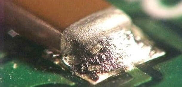
A eutectic solder alloy is a specific type of solder composition that has a unique property related to its melting point. In a eutectic alloy, the constituent elements melt and solidify at a single, well-defined temperature, without undergoing a range of phase changes or forming multiple phases during the melting or solidification process. This temperature is known as the eutectic temperature.
The term "eutectic" comes from the Greek words "eu," meaning "well," and "tektos," meaning "melted." Eutectic alloys are advantageous in soldering applications because they offer precise control over the soldering process and produce reliable, high-quality solder joints. Here are some key characteristics and advantages of eutectic solder alloys:
One of the most well-known eutectic solder alloys is the Sn63/Pb37 alloy, which consists of 63% tin (Sn) and 37% lead (Pb). This alloy has a eutectic temperature of approximately 183°C (361°F). However, it's important to note that due to environmental and health concerns, lead-based eutectic solder alloys like Sn63/Pb37 have become less common in recent years, and many industries have transitioned to lead-free solder alloys.
Lead-free eutectic solder alloys, such as SAC (Sn-Ag-Cu) alloys, have also been developed and are widely used in electronics manufacturing. These lead-free eutectic alloys offer similar benefits in terms of precise melting and solidification, but they are environmentally friendly and comply with regulations that restrict the use of lead in soldering processes.
The term "eutectic" comes from the Greek words "eu," meaning "well," and "tektos," meaning "melted." Eutectic alloys are advantageous in soldering applications because they offer precise control over the soldering process and produce reliable, high-quality solder joints. Here are some key characteristics and advantages of eutectic solder alloys:
- Sharp Melting Point: Eutectic alloys have a specific, sharp melting point, which means they transition directly from a solid to a liquid state (and vice versa) at a single temperature. This characteristic ensures that all parts of the alloy melt or solidify simultaneously, providing consistent and predictable soldering results.
- Minimal Thermal Stress: Because eutectic solder alloys melt and solidify at a single temperature, there is minimal thermal stress on the components being soldered. This reduces the risk of component damage due to rapid or uneven temperature changes.
- Less Heat-Affected Zone: Eutectic soldering often results in a smaller heat-affected zone (HAZ) around the solder joint. This is important for sensitive electronic components that can be damaged by excessive heat.
- Reliable Solder Joints: Eutectic solder joints tend to have excellent wetting properties and produce strong, reliable connections with minimal risk of voids or defects.
- Precise Soldering Process: Eutectic soldering allows for precise control over the soldering process, making it suitable for applications with tight tolerances and fine-pitch components.
One of the most well-known eutectic solder alloys is the Sn63/Pb37 alloy, which consists of 63% tin (Sn) and 37% lead (Pb). This alloy has a eutectic temperature of approximately 183°C (361°F). However, it's important to note that due to environmental and health concerns, lead-based eutectic solder alloys like Sn63/Pb37 have become less common in recent years, and many industries have transitioned to lead-free solder alloys.
Lead-free eutectic solder alloys, such as SAC (Sn-Ag-Cu) alloys, have also been developed and are widely used in electronics manufacturing. These lead-free eutectic alloys offer similar benefits in terms of precise melting and solidification, but they are environmentally friendly and comply with regulations that restrict the use of lead in soldering processes.
|
Return to home page
|
