How to Get the Best Service at Online PCB Manufacturer
|
|
WellPCB PTY LTD, registered in Australia, is a daughter company of Uniwell Circuits Co. Ltd. Focusing on Printed Circuit Board Fabrication and PCB Assembly Turnkey Services, High Quality, Low Cost, Fast Delivery, Easy Ordering for customers all over the world.

Online PCB manufacturers are proudly supplying top-quality PCB manufacturing and fabrication facilities. Their go-getting attitude is helping them keep up with the ever-evolving technology pace. But what latest equipment and system upgradations are they using?
How could you place an order on their websites and get an online quote? Why should you go for them? What kind of services should you look for in a professional online PCB manufacturer? This article will answer all these questions. Decide your favorite PCB manufacturer today! Let’s get started.
1. On the introduction of online PCB manufacturing
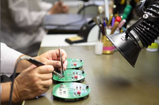
1.1 The importance of PCB manufacturing. This section describes all essential electronic circuits, including printed circuit boards (PCBs). You'll even find them in simpler products like calculators and digital clocks.
1. On the introduction of online PCB manufacturing
1.1 The importance of PCB manufacturing. This section describes all essential electronic circuits, including printed circuit boards (PCBs). You'll even find them in simpler products like calculators and digital clocks.
1.2 Why do I need to communicate with online PCB manufacturers? This section outlines the reasons for needing to communicate with online PCB manufacturers.
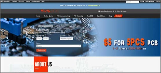
2. How to participate in the online quotation and release orders? This section discusses in detail how to get online quotes and place orders.
3. What services do you want online PCB manufacturers to offer? This section provides a detailed overview of the online PCB manufacturer's ability to offer various forms of PCB, such as multilayer, double layer, and single layer. The substrates of these PCBs are also of different types. You get rigid boards, flexible printed circuit boards, aluminum sheets, rigid-flex boards, and high-frequency boards.
4. Why choose WellPCB – an online PCB manufacturer? WellPCB is also an online PCB manufacturer. We offer all of the above services and more. Please visit our website for more information. There are a
few things that will help you understand why you are buying from us:
• WellPCB ensures high quality PCB manufacturing processes. It doesn't matter if you want a complicated design or a simple design. We are all made.
• Our technical team has many years of experience, and they regularly inspect each advanced production machine. This will ensure that your PCB quality is always unaffected.
• How do we sell cheap PCBs? If you compare it to the United Kingdom or the United States, the wages of workers in China are meager. Therefore, it gives us the advantage of producing cheap products. Moreover, this is a hint for bulk ordering PCBs, which will further reduce your costs.
• We also offer on-time and fast delivery. Our supply chain team ensures this is done.
• We can understand that you cannot trust us blindly unless you receive a satisfactory user voice. You can read their comments on our website. We have successfully served our customers from all over the world.
5. What Machinery is Used By Them?
Online PCB manufacturers these and more machines throughout the manufacturing process:
• Drilling Machines with High Precision: This makes sure the stability of the process.
• Automatic Panting Gantry Line: This makes sure copper plating quality.
• Soldering machine: For error-free soldering and moisture-free circuits.
• Text Printing Machine with high speed: This makes engraving clearer and more attractive.
• AOI Scanning Machine: For improving the reliability of PCBs.
• Flying Probe Machine with high speed: This tests for any open or short circuits.
• Laser Exposure Machine: It makes sure alignment with high precision.
Online PCB manufacturers are trying their best to deliver quality products and at an attractive price. They also provide quick delivery and low shipping rates. We know that you want to know which one of them is the best. You are curious about how the machinery they use. How you can place an order and
the services provided by them.
Hopefully, you will now be able to decide your online PCB manufacturer. If you still want to ask something or order from us, please feel free to contact us right away. Email us or give us a call.
