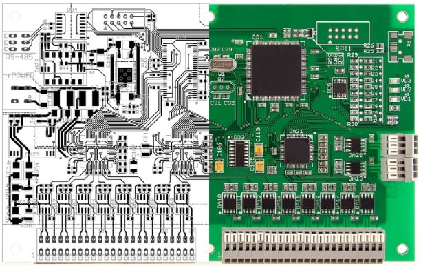
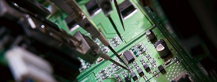
The purpose of designing a PCB assembly for manufacture is to improve the product design in three ways - quality, cost and delivery (QCD). Utilizing sound Design For Manufacture and Assembly (DFMA) practices will ensure high quality products, provide cost reductions, and shorten delivery lead times. In this day of global competition where quality, cost and speed to market are the key to a successful product, too often very simple mistakes are found late in the production process that could have been easily avoided during the design stage. With respect to the cost of a product, the majority is committed during the product design stage and so the earlier the DFMA involvement the lower the cost to implement.
Considerations
The key considerations of Design for Manufacturability are as follows:-
- Component selection
- PCB tracking design
- Via hole positioning
- PCB panel design
- Surface mount component positioning
- Component footprints and part spacing
- Incorrect pad size or design for part geometry
- Conventional component positioning
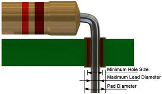
- Minimum hole size and pad diameter for component lead
- Suitability for test
Component Selection
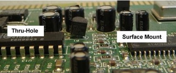
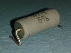
For medium to high volume PCB assembly the more of the production process that can be automated the better and so surface mount technology is preferred over conventional or through-hole technology due to it’s suitability to be easily placed by automatic machine. The image below shows a typical surface mount component along side a conventional component.
There is an increasing variety of surface mount components available on the market, with a trend of ever decreasing size. This is mainly being driven by the need to fit more components and functionality into smaller spaces – below are two images which show various surface mount components giving an idea of scale (the image on the right is of components placed on the head of a matchstick). It is important to be aware that not all components are straight forward to handle and some require specialized equipment to place.
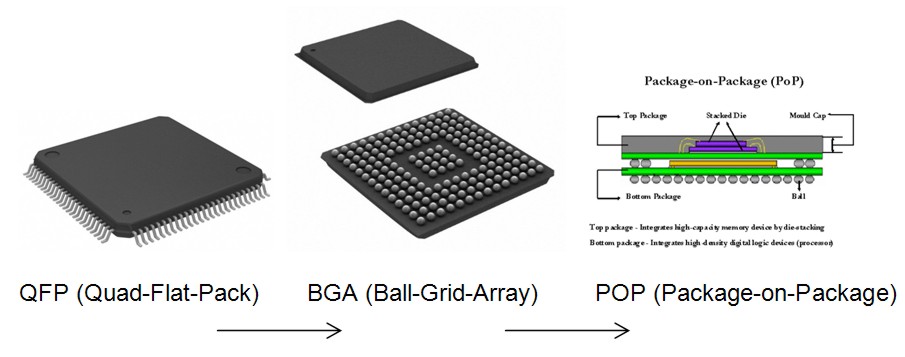
As PCB designs have gained complexity the demand for the number of connections to a device has increased as well as the demand for board space. Below are images showing how integrated circuits have evolved to first increase the number of connections to a device and then to increase the amount of functionality in a given space.
It is even more important for these type of devices to be aware that not all components are straight forward to handle and some require specialized equipment to place and inspect.
Another important aspect of component selection is to keep the number of different parts to a minimum. The reason being that the fewer different components on a design generally the lower the cost will be because of the reduced machine setup time. There will also be a reduction in the chance of error and less parts to procure. It would also be prudent at this stage to check for part obsolescence before specifying components to be used.
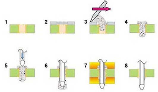
If conventional components are specified, then “pin-in-paste” or “intrusive reflow” should be considered. The diagram below shows the process of printing over the holes in the PCB, placing the component and then reflow soldering with the other surface mount parts to form the solder joints. It is very important for this process that compatible parts are selected that do not smudge the solder paste when placed and that can also withstand the reflow soldering temperatures.
|
It is possible for conventional components to have their leads 'Z-formed' to enable them to be machine placed during the surface mount assembly process. The unit cost of the parts will be higher but the assembly and soldering process will be much quicker and more repeatable.
| |||||||
PCB Tracking Design
With respect to the tracking layout within a PCB design there are aspects that should be considered specifically for manufacturability:-
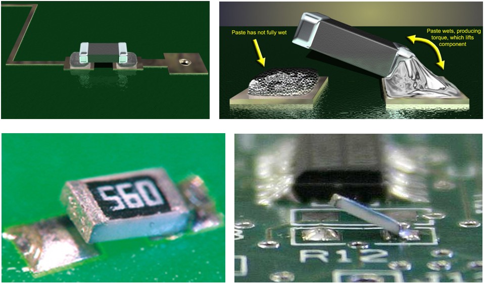
Tombstoning:- If the tracks leading to a component footprint are not thermally balanced then during the reflow soldering process one side of the component footprint will heat quicker than the other causing the solder to melt on one side first instead of at the same time. Below are some illustrations:-
Tombstoning:- If the tracks leading to a component footprint are not thermally balanced then during the reflow soldering process one side of the component footprint will heat quicker than the other causing the solder to melt on one side first instead of at the same time. Below are some illustrations:-
This can be avoided by balancing the tracks widths where possible to ensure that pads heat at the same rate. If one side is connected to a ground plane then thermal relief should be applied examples of which can be seen below:-
Copper pull-back:- All copper layers especially ground layers should not extend to the edge of the PCB design and should be pulled back from the edge to allow for ‘V grooving’ when panelising. The result of not pulling the copper back from the edge and if the PCB is panelized using ‘V grooving’ then it is possible for short circuits to occur between layers.
Via Hole Positioning
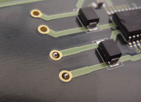
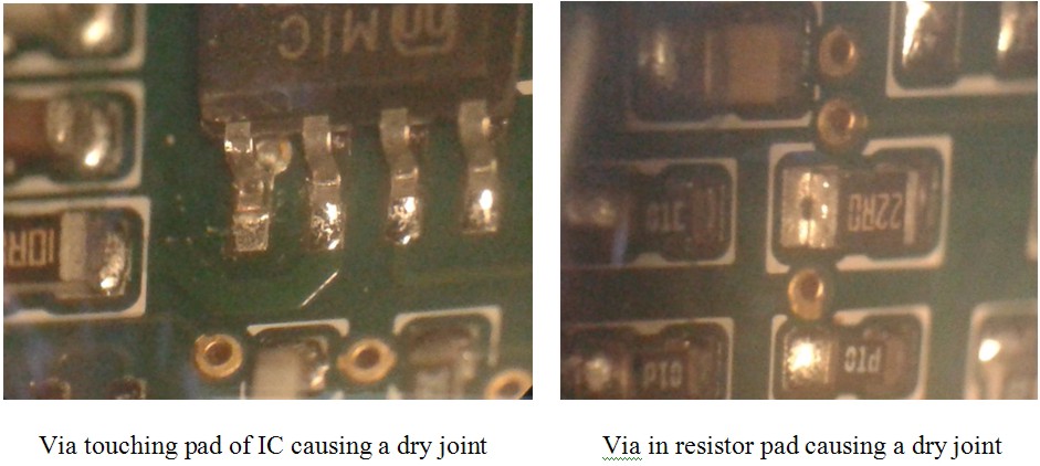
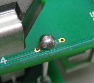
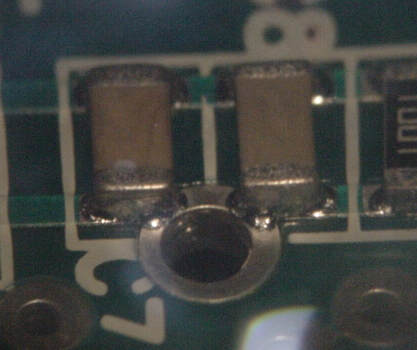
Via holes positioned in pad areas should be avoided. This can have a big impact on component solder joints during the reflow process, if the via is not isolated by solder resist, it can cause solder to wick down the hole and give a resulting dry joint – see below for two examples.
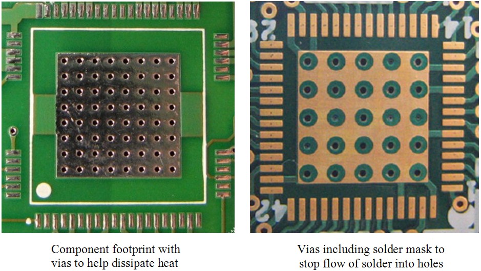
To avoid this situation vias should be positioned away from solder joints and kept separate using solder resist. There are occasions when vias are required to be incorporated within pads for thermal purposes and in these cases solder resist can be used to keep the solder from going down the holes. See below for example footprints with and without solder resist.
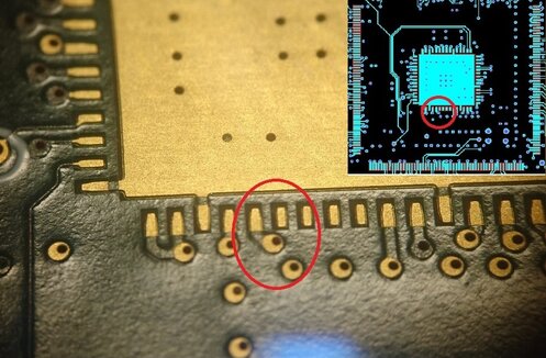
It can be useful for via's to be unmasked so they can be used for test points but when they are positioned close to component pads they do create a solder short risk - see below:-
PCB Panel Design
To allow for an efficient manufacturing process PCB designs are generally designed within a rectangular panel or frame to ensure they can be processed through the many machines that make up the surface mount assembly process – i.e. printing, placement, reflow. Depending on the size of the PCB design it may be kept to single circuit or it maybe step and repeated so multiple PCB’s can be built maximizing machine time. This has the advantage of utilizing the bare PCB material in the most efficient and cost effective way, however it also means that PCB’s should only be ordered in multiples of the panel quantity.
An effective PCB panel design would incorporate the following:-
An effective PCB panel design would incorporate the following:-
- allow for any shape PCB design to be processed
- include a minimum of two handling edges (top and bottom) to allow for components near to the edges not to be disturbed by machine PCB holding mechanism
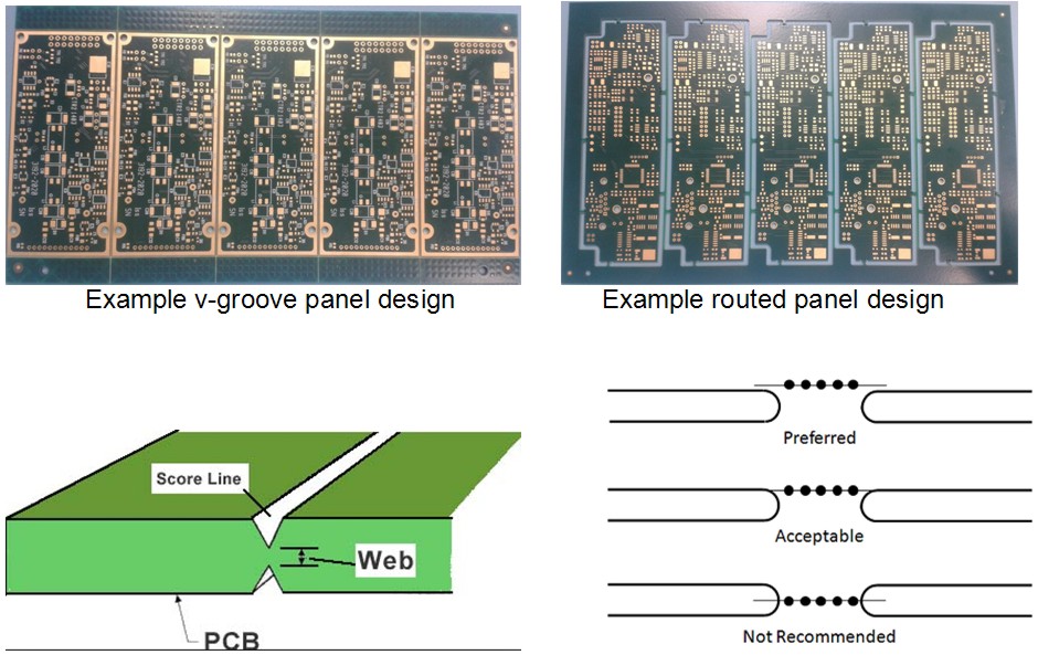
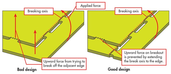
- have an acceptable method of removing PCB from the panel – either v-grooving or routing. When routing, ‘rat-bite’ breakouts are typically used.
- include a method of optically aligning PCB – Typically 3 fiducial marks
- have multiple copies of the design where appropriate
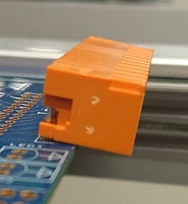
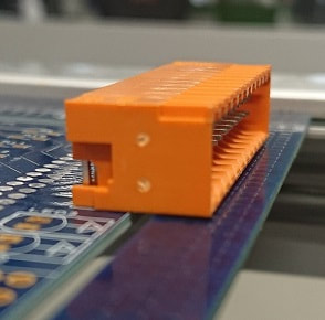
Some conventional components such as connectors need to be positioned next to the PCB edge which can cause them to be unstable and not sit flat. One solution to this problem is to design the panel in such a way to support any edge connectors before and during the soldering process - see below:-
Surface Mount Component Positioning
When positioning surface mount components it is important to have an understanding of the manufacturing process in order to keep the manufacturing cost to a minimum and reduce the chance of error. Most PCB design packages will contain design rules that govern component positioning and IPC also have developed a standard (IPC_7531) that can be a useful guide.
If the number of components is such that parts need to be mounted on both sides of the PCB then thought needs to be made to ideally position all heavy components (where total pad area to weight ratio is less than 30g per square inch) on one side of the board.
Automatic optical inspection (AOI) should also be considered to ensure as many parts as possible can be automatically inspected. All parts including their footprints should be completely visible from above so that solder joints can be inspected as well as the component body.
|
If conventional components are fitted to the opposite side of the PCB and soldered on the same side as surface mount components then clearance need to be allowed for the soldering process. If the solder joints are positioned to close to surface mount component footprints then there will be a high risk of solder short defects occurring.
|
Component Footprints and Part Spacing
All components ideally should have their own complete footprint and sufficient clearance between other parts and holes to allow independent inspection. It can be tempting design PCB's to share pads to save space as can be seen in the examples below but this causes problems for AOI to verify solder joints.
Incorrect Pad Size or Design for Part Geometry
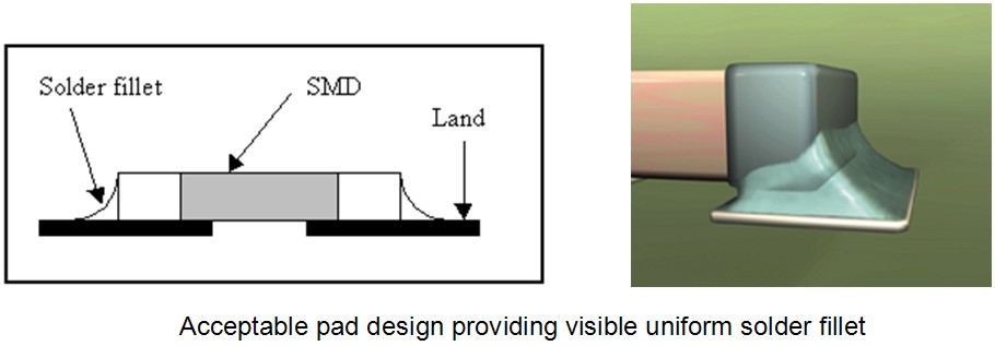
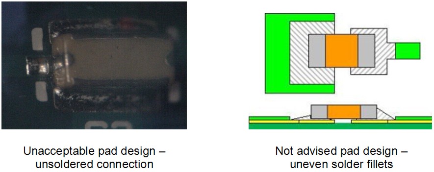
Each component to be fitted to a PCB needs to have a footprint designed that allows for a visible solder fillet to form - Document IPC_7351 can be referred to for guidance.
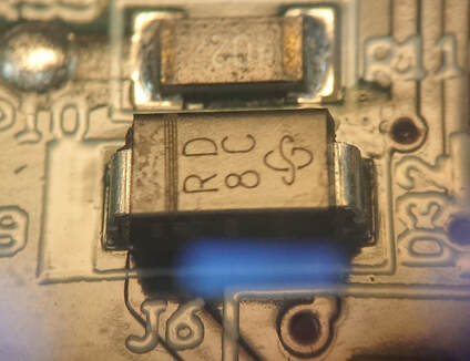
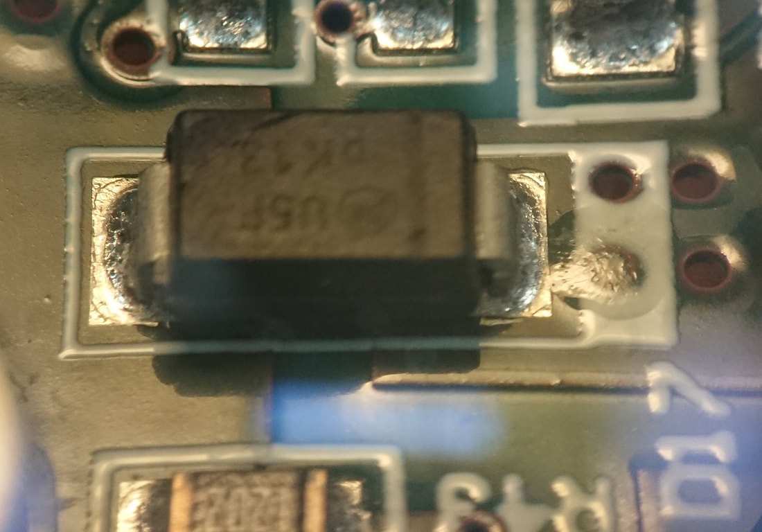
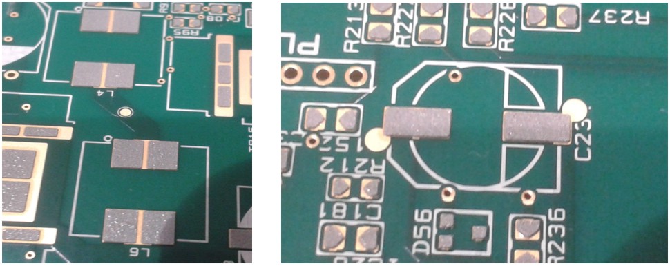
The image below on the left shows an SMD diode fitted to a footprint that doesn't conform to the component datasheet and doesn't allow automatic inspection of the solder fillets. The image on the right shows an SMD diode fitted to a footprint that does conform to the component datasheet and does allow automatic inspection of the solder fillets.
Conventional Component Positioning
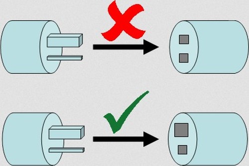
The positions of conventional or through-hole components can have a big impact on the chance of error and manufacturability of an assembly. Where possible it is recommended to position parts in a way such that an error is not possible or as unlikely as possible – Poka Yoke.
The advantages of Poka Yoke systems are as follows:-
- Minimizes or avoid risk of error
- The operator can focus on the operations that add value
- Generally easy and cheap to implement
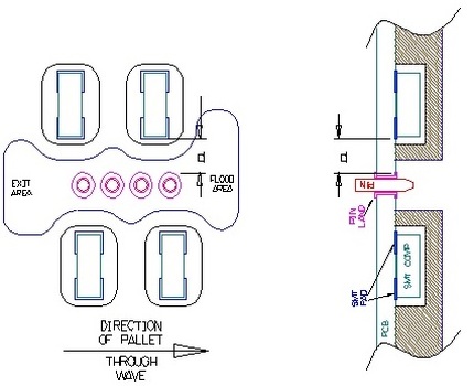
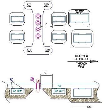
The position of conventional components in relation to surface mount is important to facilitate automation processes such as ‘wave solder’. It is important to allow enough clearance between parts to allow for tooling to be used such as wave solder pallet. The images below show how the amount of clearance required is affected by the position and orientation of components with respect to the wave. The image on the right shows that more clearance is needed when the connector orientation is perpendicular to the direction of the pallet through the wave.
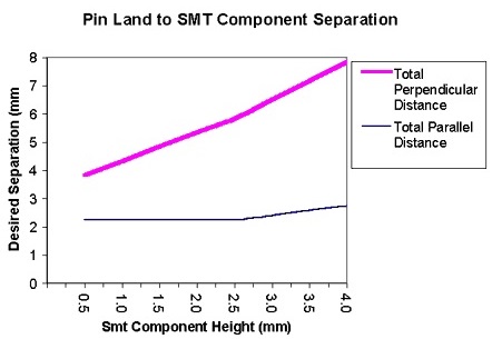
With regards to component clearances the chart to the right shows the relationship between the surface mount component height and the desired seperation.
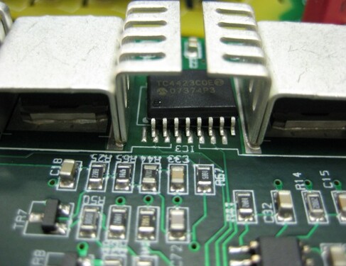
During the PCB design phase ideally give as much clearance as possible without affecting the electrical function.
During the PCB design phase ideally give as much clearance as possible without affecting the electrical function.
Minimum hole size and pad diameter for component lead
Minimum Hole Size is calculated according to equations below:
Minimum Hole Size = Maximum Lead Diameter + 0.25mm (for Level A of IPC-2222)
Minimum Hole Size = Maximum Lead Diameter + 0.20mm (for Level B of IPC-2222)
Minimum Hole Size = Maximum Lead Diameter + 0.15mm (for Level C of IPC-2222)
Calculate the Pad Diameter
After you calculate the Minimum Hole Size, you should know that the Minimum Annular Ring is
0.05mm (50um). According to IPC-2221 the Minimum Fabrication Allowance is 0.6mm for Level A, 0.5mm for Level B and 0.4mm for Level C.
Pad Diameter = Minimum Hole Size + Minimum Annular Ring X 2 + Minimum Fabrication Allowance
Pad Diameter = Minimum Hole Size + 0.1mm + 0.60mm (for Level A of IPC-2221)
Pad Diameter = Minimum Hole Size + 0.1mm + 0.50mm (for Level B of IPC-2221)
Pad Diameter = Minimum Hole Size + 0.1mm + 0.40mm (for Level C of IPC-2221)
Example: Maximum Lead Diameter = 0.55mm
According to Level A Minimum Hole Size = 0.80mm; Pad Diameter = 1.50mm
According to Level B Minimum Hole Size = 0.75mm; Pad Diameter = 1.35mm
According to Level C Minimum Hole Size = 0.70mm; Pad Diameter = 1.20mm
Suitability for Test
Testability is an important part of PCB design to ensure that ideally every part placed can be tested and verified to be correct. Certain components because of their geometry cannot be probed directly and so it is possible to either modify the footprint or to include test points within the track as can be seen below. Component testability should be considered whether the assembly is intended to be tested using a ‘bed of nails’ or flying probe tester. Boundary scan and functional testing may also be required near the final stage of release and so it is important that considerable attention is given to how this will be achieved to meet the required level of quality.

On-board IC programming can also be requirement and if so a possible solution is to include 'Tag Connect' into the PCB design. The footprint takes minimal board space, the programming lead does not need a mating connector and can only be inserted in one orientation.
Conclusion
The ultimate purpose of design for manufacture is customer satisfaction and is achieved by manufacturing with the most repeatable desired results, by standardizing the processes at the smallest cost in the shortest time.
It is important to note that this document doesn’t cover all aspects of PCB design for manufacture but does act as a guide to raise awareness of some of the important considerations that should be made during the design phase.
Surface Mount Process offers the service to provide feedback regarding design for manufacture on any products you currently have in production or are in the process of designing.
It is possible to make significant savings on assembly unit costs and also on one-off tooling costs such as stencils and support fixtures with minor changes to the design. Also, by making certain key changes it can reduce manufacturing times and so reduce the overall lead time of the product. The earlier the DFM activity takes place the easier it is to implement.
We also offer a general consultation service to discuss any particular challenge you may be facing.
If this of interest please send a message using the Contact Page
