Trapped solder paste around pads and in vias
During stencil printing, circuit boards are periodically misprinted due to clogged apertures, stencil out of alignment, solder paste rheology shifts and other issues. Stencil misprints are defined as
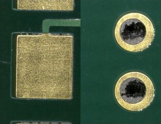
Companies commonly address the misprint by either hand wiping the misprinted side of the circuit card and/or cleaning the misprint in a stencil cleaning machine. The method of hand wiping the misprinted side of the PCB is not recommended as solder paste can be trapped in the solder mask defined channels and through-hole vias - this can be seen in the image above.
The best approach is to clean the misprinted circuit board using an automated cleaning process that provides programmable wash, rinse and dry steps. Production cleaning systems remove both wet solder paste and reflowed flux residues while meeting quality and yield objectives. To capture the wet solder paste, innovative collection and filtration systems safely capture and contain solder spheres from being sprayed onto production assemblies. Additionally, the containment and filtration systems prevent raw solder paste from entering the rinse water streams.
The printed circuit board should be cleaned as soon as possible after the mis-print to achieve the best results.
- A-Side Misprint: Initial print out of alignment with no components previously placed
- B-Side Misprint: A-Side was successfully printed and components placed and soldered. The subsequent process of printing the B-Side results in the solder paste being out of alignment resulting in a B-Side misprint
Companies commonly address the misprint by either hand wiping the misprinted side of the circuit card and/or cleaning the misprint in a stencil cleaning machine. The method of hand wiping the misprinted side of the PCB is not recommended as solder paste can be trapped in the solder mask defined channels and through-hole vias - this can be seen in the image above.
The best approach is to clean the misprinted circuit board using an automated cleaning process that provides programmable wash, rinse and dry steps. Production cleaning systems remove both wet solder paste and reflowed flux residues while meeting quality and yield objectives. To capture the wet solder paste, innovative collection and filtration systems safely capture and contain solder spheres from being sprayed onto production assemblies. Additionally, the containment and filtration systems prevent raw solder paste from entering the rinse water streams.
The printed circuit board should be cleaned as soon as possible after the mis-print to achieve the best results.
|
Return to home page
|
